Distributed feedback lasers formed via aspect ratio trapping

a feedback laser and aspect ratio technology, applied in the field of semiconductor device formation, can solve problems such as defect generation, and achieve the effects of reducing the number of gratings

Inactive Publication Date: 2008-08-07
AMBERWAVE SYST
View PDF99 Cites 112 Cited by
  • Summary
  • Abstract
  • Description
  • Claims
  • Application Information

AI Technical Summary

Benefits of technology

[0009]Another benefit is that ART patterning can provide a large refractive index difference between the dielectric material, e.g., SiO2 (1.46), and the epitaxially grown material, e.g., GaAs (3.2). This refractive index difference is larger than the refractive index difference between conventionally used materials such as GaAs and AlGaAs, and leads to a high optical coupling constant. The simplified grating formation procedure, which avoids a re-growth process, is another significant benefit in comparison to conventional methods of forming DFB structures.
[0010]The use of well de...

Problems solved by technology

These defects are generated at an interface between different materials, e.g., a III-V/Si in...

Method used


Image

  • Distributed feedback lasers formed via aspect ratio trapping
  • Distributed feedback lasers formed via aspect ratio trapping
  • Distributed feedback lasers formed via aspect ratio trapping

Examples


Embodiment Construction

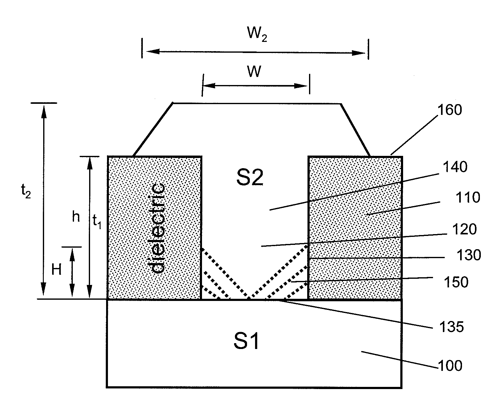
[0023]Referring to FIG. 1, a method for forming a relatively low defect or defect-free semiconductor material on a lattice-mismatched substrate is illustrated. A substrate 100 includes a first crystalline semiconductor material S1. The substrate 100 may be, for example, a bulk silicon wafer, a bulk germanium wafer, a semiconductor-on-insulator (SOI) substrate, or a strained semiconductor-on-insulator (SSOI) substrate. The substrate 100 may include or consist essentially of the first semiconductor material S1, such as a group IV element, e.g., germanium or silicon. In an embodiment, substrate 100 includes or consists essentially of n-type (100) silicon. The substrate 100 may include a material having a first conductivity type, e.g., n+Si.

[0024]A dielectric layer 110 is formed over the semiconductor substrate 100. The dielectric layer 110 may include or consist essentially of a dielectric material, such as silicon nitride or silicon dioxide. The dielectric layer 110 may be formed by a...


PUM


Abstract

Structures including dielectric diffraction gratings. In some embodiments, laser devices include diffraction gratings defined by openings formed in a dielectric material.

Description

RELATED APPLICATION[0001]This application claims priority to U.S. Provisional Patent Application Ser. No. 60 / 852,781, filed Oct. 19, 2006, the disclosure of which is hereby incorporated by reference in its entirety.FIELD OF THE INVENTION[0002]This invention relates generally to semiconductor processing and particularly to formation of light-emitting devices based on lattice-mismatched semiconductor structures.BACKGROUND[0003]Distributed feedback (DFB) lasers with stable longitudinal single-mode operation are critical for applications such as optical-information processing, interferometric measuring, holographic printing, optical gas sensing, atomic spectroscopy and medical diagnoses. Examples of various DFB lasers are shown and described in U.S. Pat. Nos. 5,295,150 and 5,953,361 and articles such as Japanese Journal of Applied Physics, Vol. 43, No. 4B, 2004, pp. 2019-2022, Japanese Journal of Applied Physics Vol. 44, No. 4B, 2005, pp. 2546-2548, and Journal of Crystal Growth 261 (20...

Claims


Application Information

Patent Timeline
IPC IPC(8): H01S5/12H01L21/02H01L33/00H01L33/12
CPCH01L21/02381H01L33/08H01L21/02538H01L21/02546H01L21/02573H01L21/0262H01L21/02639H01L21/02647H01L33/0066H01L33/12H01S5/0207H01S5/223H01S5/2234H01S5/227H01S5/3202H01L33/16H01L21/02524H01S2304/12H01S5/021H01S5/0218H01S5/2237H01L33/20H01L33/24H01L33/06H01L33/007H01L33/0087H01S5/24H01L33/0093
Inventor LI, JIZHONG
Owner AMBERWAVE SYST
Why Eureka
Try Eureka