Method for manufacturing semiconductor substrate

a manufacturing method and semiconductor technology, applied in the direction of semiconductor devices, basic electric elements, electrical apparatus, etc., can solve the problems of increasing manufacturing costs, difficult to sufficiently reduce the introduction of lattice defects, and the technique cannot be regarded as suitable for industrial production methods, etc., to achieve the effect of simple techniqu

Active Publication Date: 2008-08-14
SHIN ETSU CHEM IND CO LTD
View PDF5 Cites 74 Cited by
  • Summary
  • Abstract
  • Description
  • Claims
  • Application Information

AI Technical Summary

Benefits of technology

[0009]The present invention was accomplished in view of these problems. The object of the invention is to provide a method for manufacturi...

Problems solved by technology

This technique, however, requires the epitaxial growth of Si1-xGex many times, and hence increases the manufacturing costs.
Most of all, it is difficult to sufficiently reduce the lattice defects introduced in the Ge epitaxial layer.
Moreover, the technique entails a heat treatment subsequent to delamination in order to increase the bonding strength of the bonding interface between the support substrate and the Ge layer, in whic...

Method used


Image

  • Method for manufacturing semiconductor substrate
  • Method for manufacturing semiconductor substrate
  • Method for manufacturing semiconductor substrate

Examples


first embodiment

(GeOI Substrate)

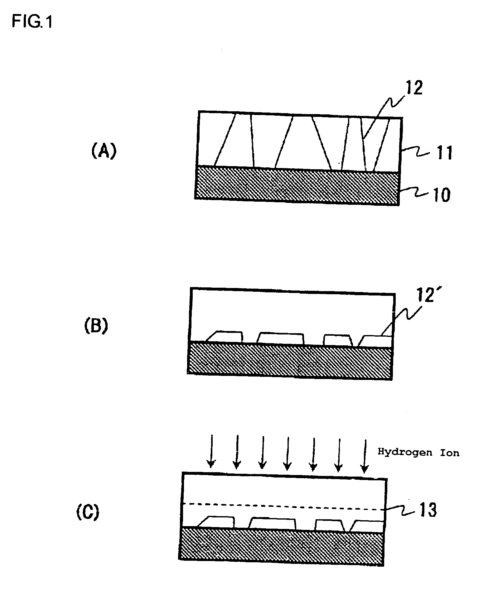
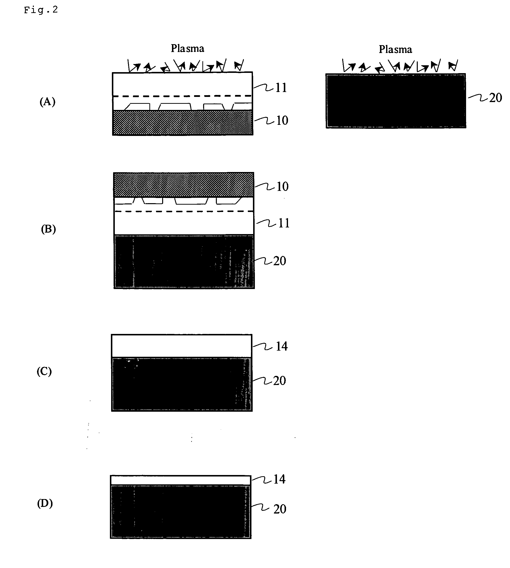
[0022]FIGS. 1 (A) to (C) and FIGS. 2 (A) to (D) are flowcharts for explaining an example of a process for manufacturing a semiconductor substrate according to the present invention. In this embodiment, an example of a process for manufacturing a GeOI substrate is explained. In each of these flowcharts, reference numeral 10 denotes a silicon (Si) substrate for epitaxially growing germanium (Ge) by a chemical vapor deposition (CVD) method. The Si substrate 10 is, for example, a generally commercially available Si substrate grown by the CZ (Czochralski) method. The electrical properties of the Si substrate, such as the conductivity type, an electrical characteristic value such as specific resistivity and the like, as well as the crystal orientation and the crystal size thereof are suitably selected depending on the device design values, the process, and the like of the device to which the Ge epitaxial film produced in the method of the present invention is applied.

[0023...

second embodiment

(SGOI Substrate)

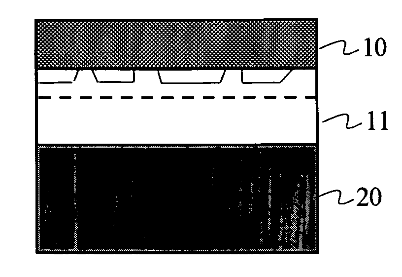
[0033]The second embodiment describes an example of a process for manufacturing a SGOI substrates. Since the process is basically the same as that described in the first embodiment, it will be explained again with reference to FIGS. 1 (A) to (C) and FIGS. 2 (A) to (D). In this embodiment, reference numeral 11 in the figures denotes a SiGe epitaxial film obtained by epitaxial growth of silicon germanium (SiGe) by a chemical vapor deposition (CVD) method.

[0034]Also in the SiGe epitaxial film 11, high-density defects (threading dislocations) 12 are introduced from the interface between the SiGe epitaxial film 11 and the Si substrate 10 (FIG. 1 (A)). In order to gather the dislocations in the SiGe epitaxial film 11 near the interface of the epitaxial film 11 and the Si substrate 10 (denoted by reference numeral 12′), a heat treatment is performed at a temperature of not less than 650° C. and not more than 1200° C. (preferably not less than 700° C. and not more than 1200°...


PUM


Abstract

To obtain a semiconductor substrate having a high-quality Ge-based epitaxial film in a large area, a SiGe mixed crystal buffer layer and a Ge epitaxial film is grown on a main surface of a Si substrate 10. Although high-density defects are introduced in the Ge epitaxial film 11 from an interface between the Ge epitaxial film 11 and the Si substrate 10, the Ge epitaxial film is subjected to a heat treatment at a temperature of not less than 700° C. and not more than 900° C. to cause threading dislocations 12 to change into dislocation-loop defects 12′ near the interface between the Ge epitaxial film 11 and the Si substrate. A main surface of at least one of the Ge epitaxial film 11 with an ion implanted layer and a support substrate 20 is then subjected to a plasma treatment or ozone treatment for the purpose of surface cleaning, surface activation, and the like, after which the main surfaces of the Ge epitaxial film 11 and the support substrate 20 are appressed against and bonded to each other with their surfaces being determined as the joint surfaces. An external impact is then applied to the bonding interface, causing the Ge epitaxial film to be delaminated along a hydrogen ion implanted interface 13, thus obtaining a Ge thin film 14. A surface of the Ge thin film 14 is subsequently subjected to a final surface treatment (for example, CMP) to remove the damage caused by the hydrogen ion implantation, thus resulting in a GeOI substrate having the Ge thin film 14 on the surface thereof.

Description

BACKGROUND OF THE INVENTION[0001]1. Field of the Invention[0002]The present invention relates to a method for manufacturing a semiconductor substrate comprising a germanium-based epitaxial film such as germanium (Ge), silicon germanium (SiGe) or the like on a foreign substrate.[0003]2. Description of the Related Art[0004]While the use of SOI (Silicon-On-Insulator) substrates has previously been known as a technique of increasing the carrier mobility in semiconductor devices to enhance the processing speed, the use of GeOI (Germanium-On-Insulator) substrates has recently been proposed. The reason is that the carrier mobility in the Ge crystal is higher than that in the Si crystal, with the electron mobility being about twice higher, and the hole mobility being about four times higher, which is advantageous for designing high-speed operating semiconductor devices.[0005]To epitaxially grow a Ge film on a foreign substrate, one technique is known which comprises depositing on a Si subst...

Claims


Application Information

Patent Timeline
IPC IPC(8): H01L21/20
CPCH01L21/02381H01L21/0245H01L21/76254H01L21/0262H01L21/02532
Inventor AKIYAMA, SHOJIKUBOTA, YOSHIHIROITO, ATSUOTANAKA, KOICHIKAWAI, MAKOTOTOBISAKA, YUUJI
Owner SHIN ETSU CHEM IND CO LTD
Why Eureka
Try Eureka