

Method for forming metal silicide layer
- Summary
- Abstract
- Description
- Claims
- Application Information
AI Technical Summary
Benefits of technology
Problems solved by technology
Method used
Image

Examples
Embodiment Construction
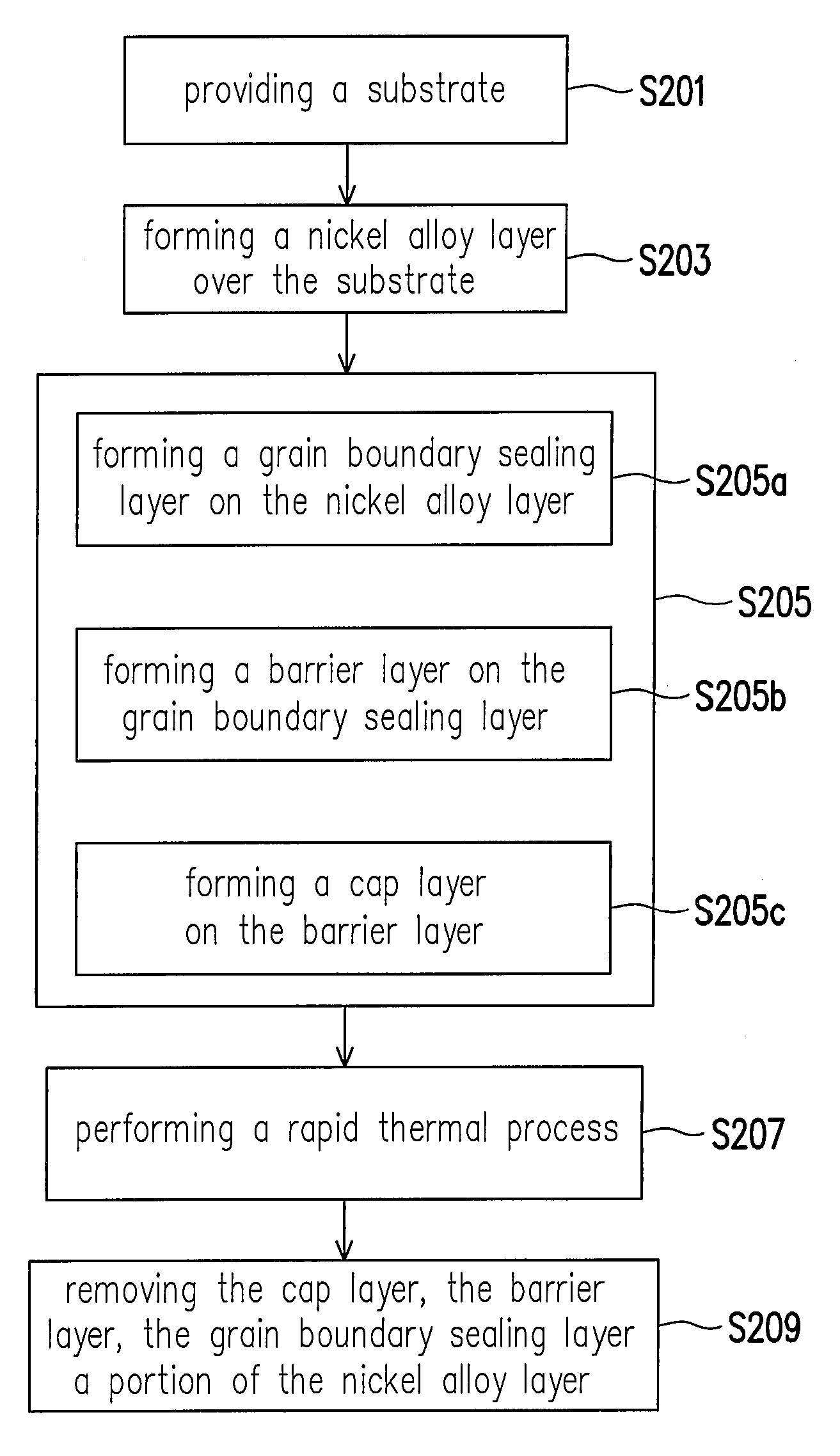
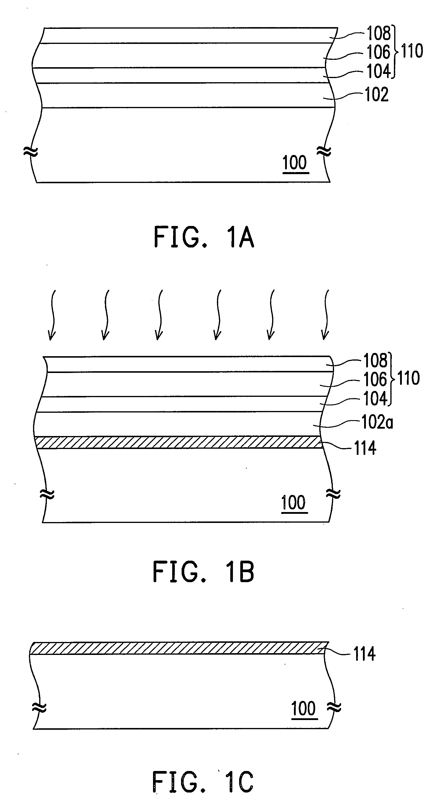
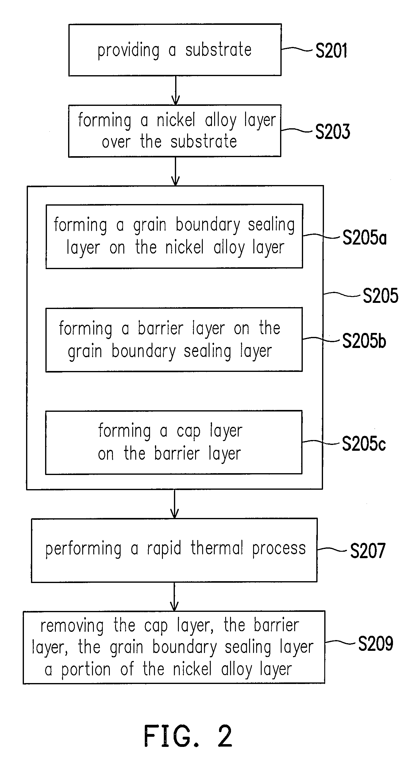
[0033]FIGS. 1A through 1C are cross-sectional views showing a method for forming a metal silicide layer according to a preferred embodiment of the invention. FIG. 2 is a process flow showing a method for forming a metal silicide layer according to one embodiment of the present invention. As shown in FIG. 1A and FIG. 2, in the step S201, a substrate 100 is provided. The substrate 100 has at least one semiconductor device (not shown) formed thereon. Then, in the step S203, a nickel alloy layer 102 is formed over the substrate 100. The nickel alloy layer 102 can, for example, contain the noble metal selected from a group consisting of Pt, Pd, Mo, Ag, Au and the combination thereof. That is, the nickel alloy layer 102 can be a nickel-noble metal layer. Furthermore, the weight percentage of the noble metal in the nickel alloy layer is about 5˜10%. Moreover, the method for forming the nickel alloy layer 102 can be the conventional deposition process such as chemical vapor deposition.
[0034...
PUM
 Abstract
Description
Claims
Application Information