

Plasma etching method
a technology of etching method and plasma, which is applied in the direction of fluid pressure measurement, instruments, vacuum gauges, etc., can solve the problems of slowing down the etching rate, extremely sparse region, and inability to accurately detect the depth of the via-hol
- Summary
- Abstract
- Description
- Claims
- Application Information
AI Technical Summary
Benefits of technology
Problems solved by technology
Method used
Image

Examples
text example 3
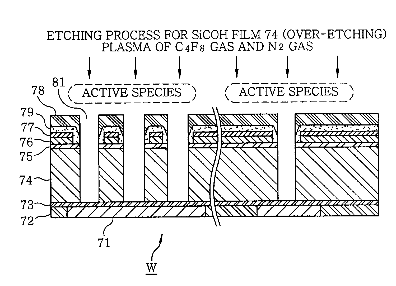
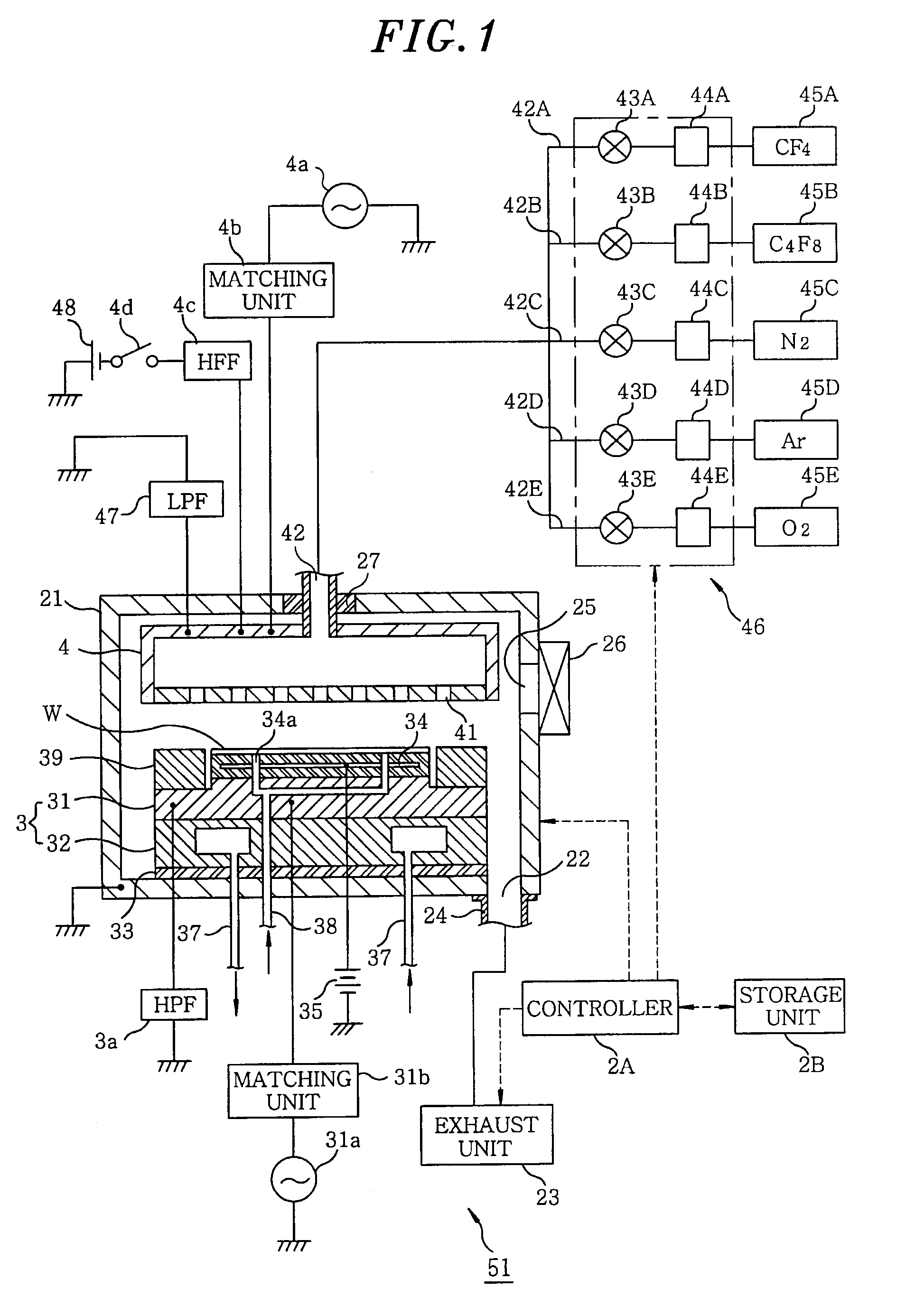
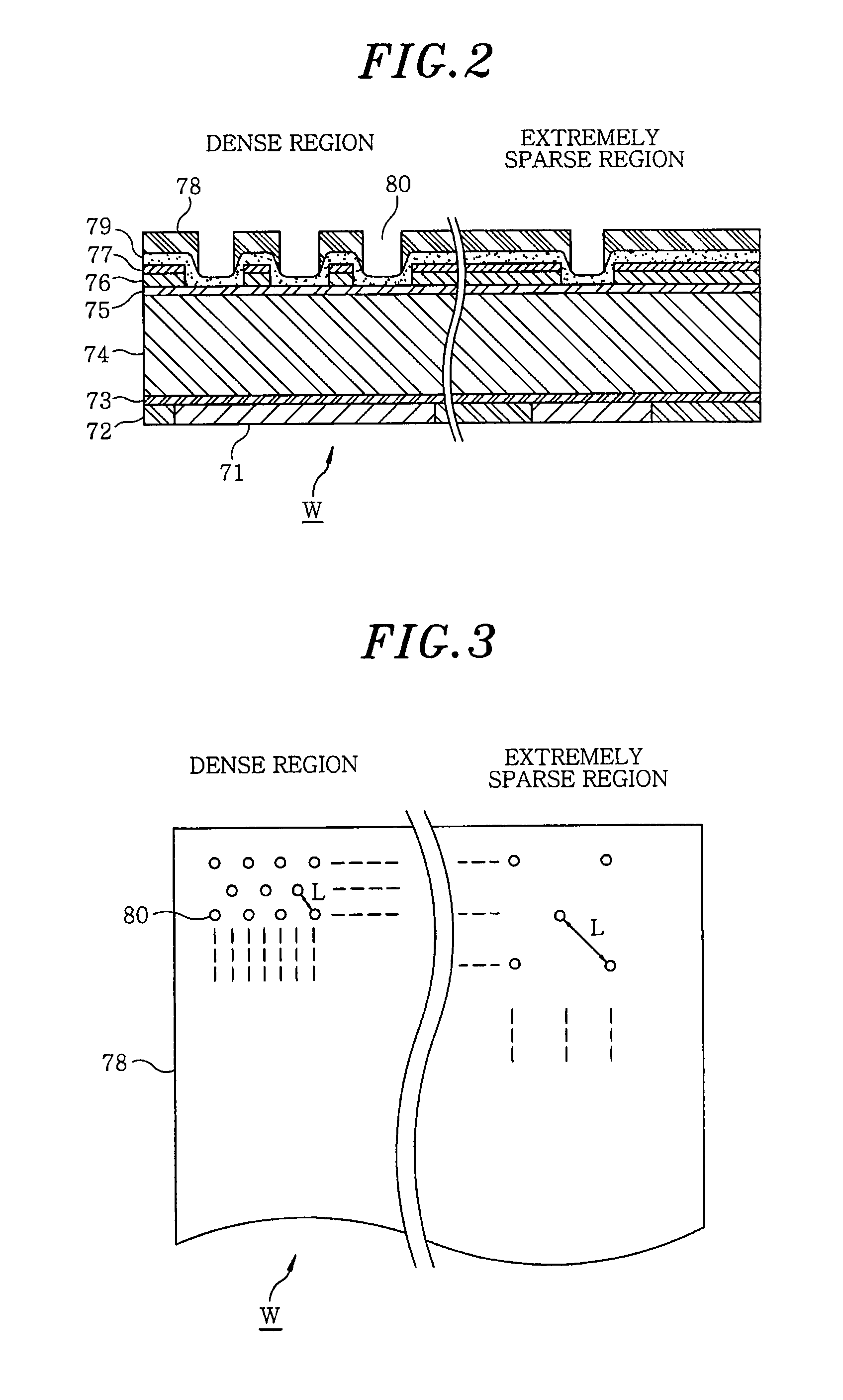
[0105]In order to check whether the same effect as the present invention can be obtained in case of changing the processing conditions for the over-etching without applying a negative DC voltage to the upper electrode 4, a test was performed on the same wafer W as in text example 1 under the processing conditions described later. Herein, the test was performed under the conditions such that the via-hole 81 was formed to the top surface of the SiCN film 73 in the extremely sparse regions where the gap L between the adjacent via-holes 81 is 10 μm or more, and the via-hole 81 did not penetrate the SiCN film 73 in the dense regions and the sparse regions. Then, the dense regions and the sparse regions were observed. In the following conditions, those same as test example 1-1 are omitted.
Processing Conditions
PUM
| Property | Measurement | Unit |
|---|---|---|
| distance | aaaaa | aaaaa |
| distance | aaaaa | aaaaa |
| relative permittivity | aaaaa | aaaaa |
Abstract
Description
Claims
Application Information