Silicone coating composition

a technology of silicon coating and composition, applied in the direction of diffusion transfer process, instruments, photosensitive materials, etc., can solve the problems of uneven exposure of photoresist, standing wave effect, and less suitable in the futur

Active Publication Date: 2008-08-21
MERCK PATENT GMBH
View PDF99 Cites 41 Cited by
  • Summary
  • Abstract
  • Description
  • Claims
  • Application Information

AI Technical Summary

Problems solved by technology

Silicon dioxide has been employed within the industry as a dielectric material for the manufacture of devices for nearly three decades, but may become less suitable in the future because of its relatively high dielectric constant (k˜4.1).
Additionally, in current conventional semiconductor manufacturing, in order to prevent light reflection from being transmitted through the photo-resist, reflected off the substrate and back into the photoresist, where it can interfere with incoming light and so result in the uneven exposure of the photoresist, conventionally one or more antireflective layers may be deposited before the photoresist is deposited or spun on.
In the absence of an antireflection coating, interference of reflected and incident exposure radiation can cause standing wave effects that distort the uniformity of the radiation through the thickness of the photoresist layer.
Variations in reflectivity throughout the entire imaged areas can cause undesirable line width variation for features which are designed to have similar dimensions.

Method used


Image

  • Silicone coating composition
  • Silicone coating composition
  • Silicone coating composition

Examples


synthesis example 1

[0032]180 grams of methyltrimethoxysilane, 120 grams of 2-cyanoethyltriethoxysilane, 36 grams of phenyltrimethoxysilane and 270 grams of glacial acetic acid were charged into a 2L flask equipped with a thermometer, a cold water condenser and a mechanical stirrer. After the reaction mixture was heated to 80° C., 4 grams of para-toluenesulfonic acid monohydrate dissolved in 31 grams of acetic acid was added. The reaction was maintained at reflux for 17 hrs and then allowed to cool to room temperature. After the reaction solution was cooled to room temperature, the solution was filtered and the filtrate was slowly poured into DI water with stirring, causing polymer to precipitate. The precipitated polymer was filtered, thoroughly washed with DI water and dried at room temperature. FTIR showed that the polymer contained SiOH groups. The polymer was found to be soluble in most organic solvents. However, the polymer became insoluble once dried at elevated temperatures due to further conde...

synthesis example 2

[0033]30.2 grams of polymer from Synthesis Example 1 was dissolved in 100 grams of acetone in a 500 mL flask equipped with a thermometer, a cold water condenser and a mechanical stirrer. 16.5 grams of bischloromethyltetramethyldisiloxane and 2.67 grams of 3-cyanopropyldimethylchlorosilane were added and the reaction mixture was refluxed for 16 hrs. The solution was then allowed to cool to room temperature. The cooled solution was then poured into hexane with stirring, causing polymer to precipitate. The polymer obtained was dissolved in acetone, filtered and precipitated in DI water. The polymer obtained was filtered and washed thoroughly with DI water. The polymer (20 g) was finally dried in a vacuum oven at 45° C. for 2 days. FTIR did not detect SiOH groups in the polymer. 1H NMR showed that the polymer contained no SiOCH2CH3 or SiOCH3 groups. The polymer was found soluble in most organic solvents. The polymer had a Mw of 8303 g / mol and Mn of 3301 g / mol.

synthesis example 3

[0034]70 grams of methyltrimethoxysilane, 30 grams of 3-chloropropyltrimethoxysilane, 14.2 grams of phenyltrimethoxysilane and 108 grams of glacial acetic acid were charged into a 2L flask equipped with a thermometer, a cold water condenser and a mechanical stirrer. After the reaction mixture was heated to 80° C., 1.4 grams of para-toluenesulfonic acid monohydrate was added. The reaction was maintained at refluxing for 16 hrs and then allowed to cool to room temperature. After the reaction solution was cooled to room temperature, the solution was filtered and the filtrate was slowly poured into DI water with stirring, causing polymer to precipitate. The precipitated polymer was filtered, thoroughly washed with DI water and dried at room temperature. FTIR showed that the polymer contained SiOH groups. The polymer was found to be soluble in most organic solvents. However, the polymer became insoluble once dried at elevated temperatures due to further condensation of SiOH groups.

SYNTHE...


PUM

PropertyMeasurementUnit
temperatureaaaaaaaaaa
thicknessaaaaaaaaaa
temperatureaaaaaaaaaa

Abstract

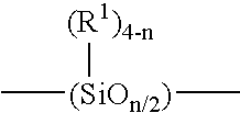
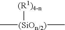
The present invention relates to a composition comprising:(a) a polymer having at least one repeating unit of formulawhere R1 is a non-hydrolysable group and n is an integer ranging from 1 to 3; and (b) a crosslinking catalyst. The composition is useful in forming low k dielectric constant materials and as well as hard mask and underlayer materials with anti-reflective properties for the photolithography industry.

Description

BACKGROUND OF THE INVENTION[0001]This invention relates generally to high silicon-content resin composition that can be used to form thin film thermosets, useful in forming low k dielectric constant materials and as well as hard mask and underlayer materials with anti-reflective properties for the photolithography industry.[0002]As the dimensions of microelectronic devices become smaller, the importance of fully exploiting the physical properties of the materials used in their manufacture becomes more essential. This is particularly true of the dielectric materials that are used to insulate metal lines, vias and electronic components from one another because of the contributions to capacitance that these materials make. Silicon dioxide has been employed within the industry as a dielectric material for the manufacture of devices for nearly three decades, but may become less suitable in the future because of its relatively high dielectric constant (k˜4.1). Recently, however, siloxanes...

Claims


Application Information

Patent Timeline
Patent Type & Authority Applications(United States)
IPC IPC(8): G03C1/46C04B28/26G03C8/00C08G77/20
CPCC09D183/04C08G77/06C09D183/06
Inventor WU, HENGPENGKIM, WOOKYUZHUANG, HONGLU, PINGHUNGNEISSER, MARKABDALLAH, DAVIDZHANG, RUZHI
Owner MERCK PATENT GMBH
Why Eureka
Try Eureka