Compound semiconductor device and method of manufacturing the same

a semiconductor and compound technology, applied in the direction of semiconductor devices, basic electric elements, electrical equipment, etc., can solve the problems of difficult control of insulation properties, high cost of semi-insulating sic substrate used as a substrate of high frequency devices, and affecting the spread of gan-hem

Active Publication Date: 2008-08-21
FUJITSU LTD
View PDF28 Cites 58 Cited by
  • Summary
  • Abstract
  • Description
  • Claims
  • Application Information

AI Technical Summary

Benefits of technology

[0017]According to one aspect of an embodiment, a compound semiconductor device has a buffer layer formed on a conductive SiC substrate, an AlxGa1-xN layer formed on the buffer layer in which an impurity for reducing carrier concentration from an unintentionally doped donor impurity, is added and in which the Al composition x is 0≦x≦1, a GaN-based carrier transit layer formed on the AlxGa1-N layer, a carrier supply layer formed on the carrier transit layer, a source electrode and a drain electrode formed on the carrier supply layer, and a gate electrode formed on the carrier supply layer between the source electrode and the drain electrode.
[0018]According to another aspect of an embodiment, a method of manufacturing a compound semiconductor device in the present invention includes: forming a buffer layer on the conductive SiC substrate; forming an AlxGa1-xN layer on the buffer layer in which an impurity for reducing carrier concentration from an unintentionally doped donor impurity is added and in which the Al composition x is 0≦x≦1, forming a GaN-based carrier transit layer on the AlxGa1-xN layer; forming the carrier supply layer on the carrier transit layer; forming the source electrode and the drain electrode on the carrier supply layer; forming a gate electrode on the carrier supply layer between the source electrode and the drain electrode.

Problems solved by technology

However, the cost of a semi-insulating SiC substrate used as a substrate of a high frequency device is very high with the reason that the control of insulation properties is difficult, etc.
Because of this, there is a possibility that the spread of GaN-HEMT may be hindered if the semi-insulation SiC substrate is used.
However, a large unevenness is often generated on the growth surface of the AlN layer formed with the HVPE method.
In the case of forming a compound semiconductor layer containing a GaN layer on an AlN layer having a surface with such large unevenness and configuring an electron device such as HEMT, sufficient device characteristics can not be obtained.

Method used


Image

  • Compound semiconductor device and method of manufacturing the same
  • Compound semiconductor device and method of manufacturing the same
  • Compound semiconductor device and method of manufacturing the same

Examples


Embodiment Construction

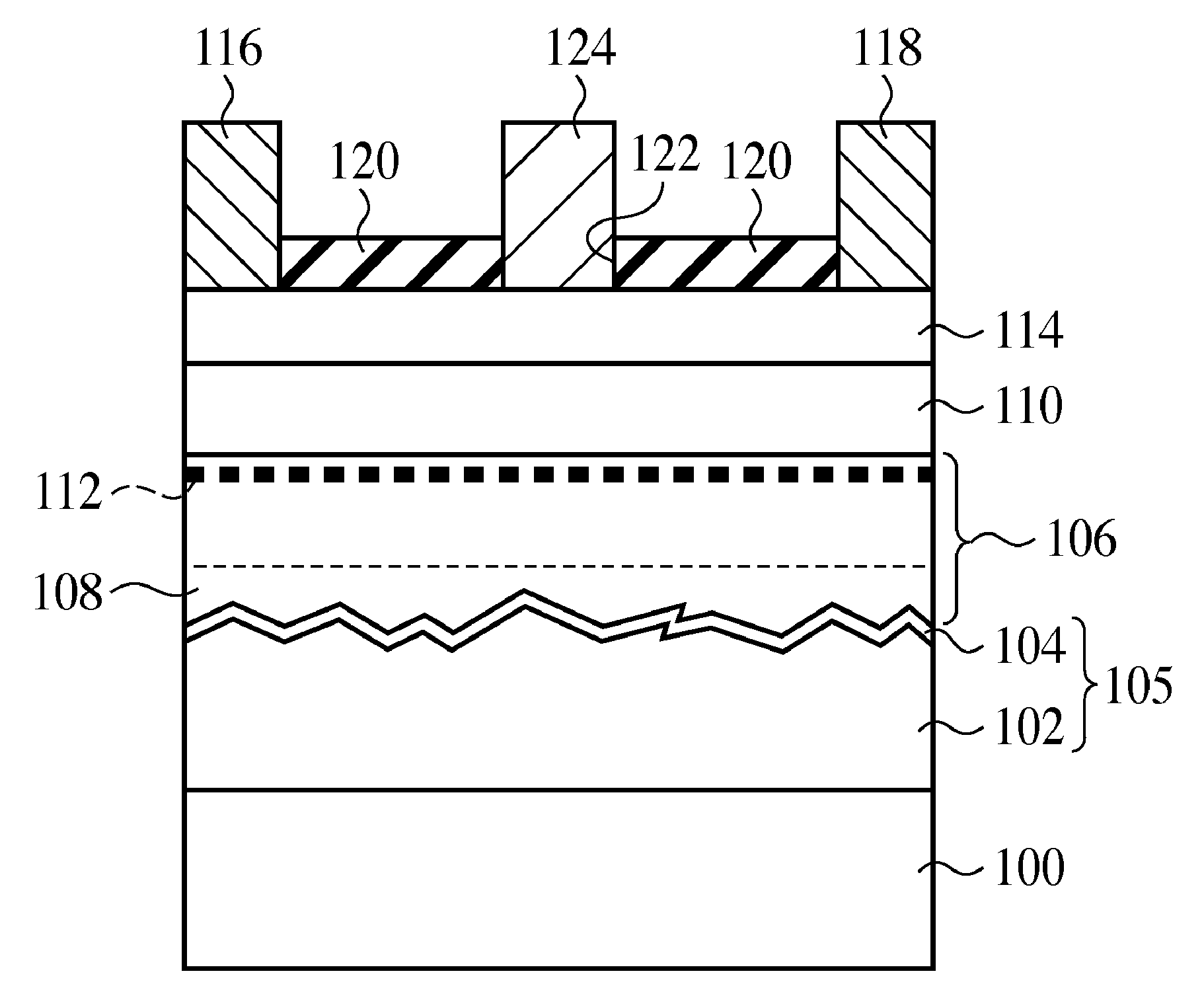
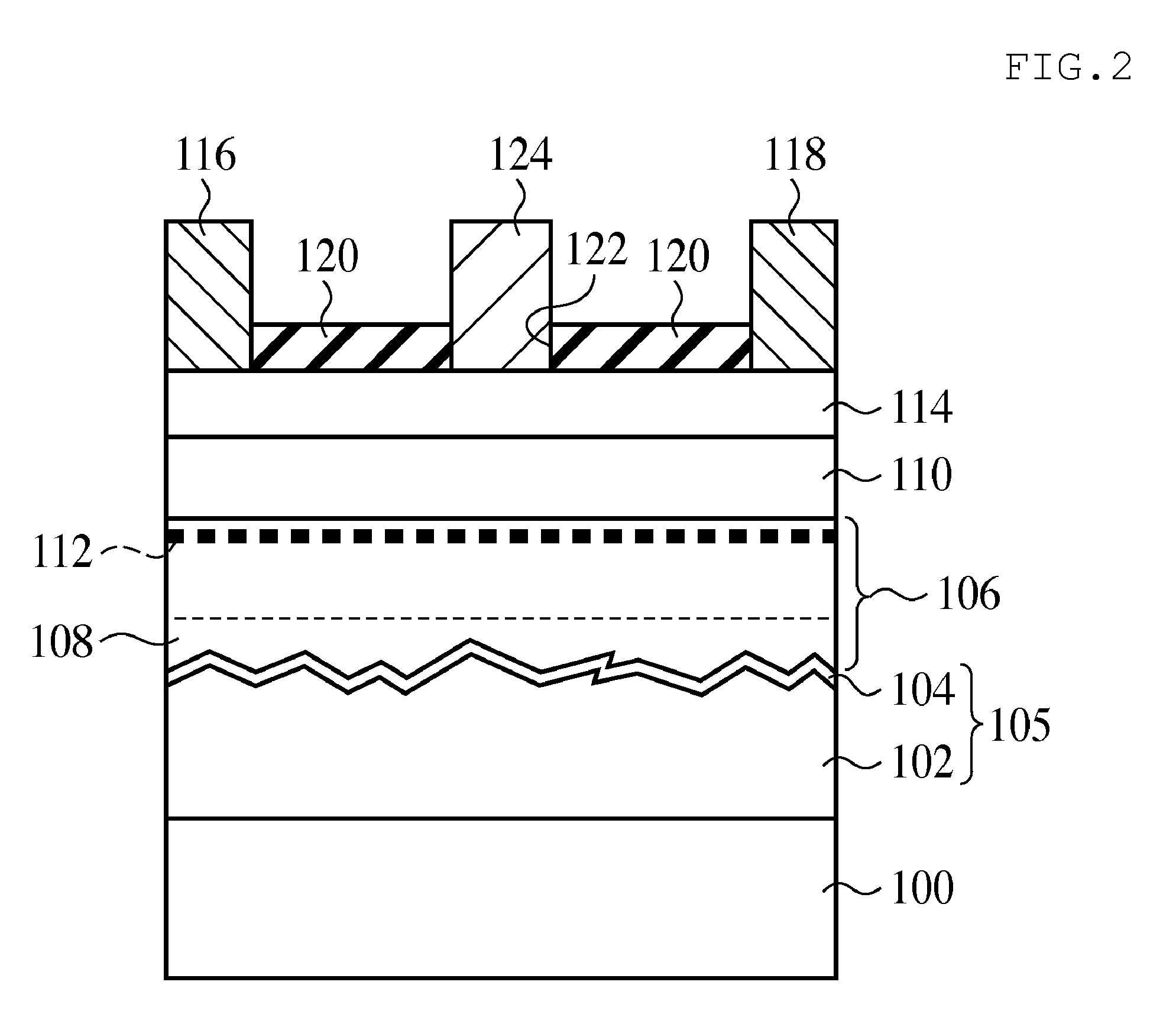
[0030]FIG. 2 is a structure of the GaN-HEMT in which a GaN layer is simply formed on an AlN buffer layer.

[0031]As shown in the figure, an undoped i-type AlN buffer layer 102 of 25 μm thickness is formed on a single crystal n-type conductive SiC substrate 100. The i-type AlN buffer layer 102 is, as described later, formed with an HVPE method, and a large unevenness is generated on its surface.

[0032]An undoped i-type AlN layer 104 of 0.1 μm thickness or less, specifically about 50 nm thickness, is formed on the i-type AlN buffer layer 102. Because of the large unevenness on the surface of the i-type AlN buffer layer 120, a large unevenness is generated also on the surface of the relatively thin i-type AlN layer 104.

[0033]In this way, a buffer layer 105 composed of the i-type AlN buffer layer 102 and the i-type AlN layer 104 is formed on the n-type conductive SiC substrate 100.

[0034]An undoped i-type GaN layer 106 of 1 to 2 μm thickness is formed on the i-type AlN layer 104. A low resi...


PUM


Abstract

A compound semiconductor device has a buffer layer formed on a conductive SiC substrate, an AlxGa1-xN layer formed on the buffer layer in which an impurity for reducing carrier concentration from an unintentionally doped donor impurity is added and in which the Al composition x is 0<x<1, a GaN-based carrier transit layer formed on the AlxGa1-xN layer, a carrier supply layer formed on the carrier transit layer, a source electrode and a drain electrode formed on the carrier supply layer, and a gate electrode formed on the carrier supply layer between the source electrode and the drain electrode. Therefore, a GaN-HEMT that is superior in device characteristics can be realized in the case of using a relatively less expensive conductive SiC substrate compared with a semi-insulating SiC substrate.

Description

CROSS-REFERENCE TO RELATED APPLICATION[0001]This application is based upon and claims the benefit of priority from the prior Japanese Patent Application No. 2007-038905 filed on Feb. 20, 2007, the entire contents of which are incorporated herein by reference.BACKGROUND OF THE INVENTION[0002]1. Field of the Invention[0003]The present invention relates to a compound semiconductor device and a method of manufacturing the same.[0004]2. Description of Related Art[0005]Recently, development of an electron device has been performed actively in which, on a substrate made of sapphire, silicon carbide (SiC), gallium nitride (GaN), silicon (Si) and the like, the crystal growth of an aluminum gallium nitride (AlGaN) / GaN hetero structure is performed and a GaN layer is included as an electron transit layer. For example, a high electron mobility transistor (HEMT) is known as such an electron device. The band gap of GaN is 3.4 eV and is large compared with 1.4 eV of GaAs. Because of this, GaN is e...

Claims


Application Information

Patent Timeline
Patent Type & Authority Applications(United States)
IPC IPC(8): H01L29/267H01L21/338
CPCH01L21/02378H01L29/2203H01L21/02458H01L21/02494H01L21/02505H01L21/0254H01L21/02581H01L21/0262H01L29/107H01L29/1608H01L29/2003H01L29/267H01L29/66462H01L29/7786H01L29/812H01L29/66431H01L21/02425
Inventor IMANISHI, KENJIKIKKAWA, TOSHIHIDE
Owner FUJITSU LTD
Why Eureka
Try Eureka