

Method for Forming Multi-Layered Binary Oxide Film for Use in Resistance Random Access Memory
a technology of binary oxide film and resistance random access memory, which is applied in the direction of oxygen/ozone/oxide/hydroxide, chemistry apparatus and processes, material nanotechnology, etc., can solve the problems of limited dram scale-down (decrease in gate length), the inability to ensure sufficient device margin when operating at low voltage, and the inability to meet the requirements of low-voltage research. , to achieve the effect of excellent reproducibility and effective mass production
- Summary
- Abstract
- Description
- Claims
- Application Information
AI Technical Summary
Benefits of technology
Problems solved by technology
Method used
Image

Examples
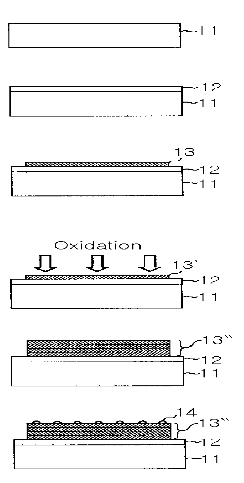
example 1
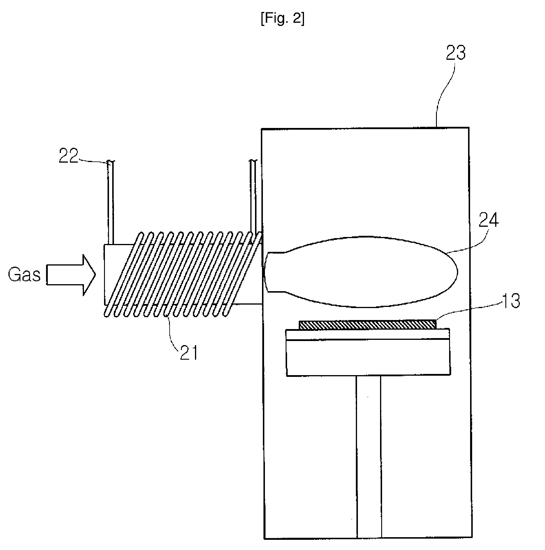
[0046]An Al thin film was grown in a thickness of 30 Å on a Pt lower electrode layer formed on a Si substrate. Using the apparatus shown in FIG. 2, Ar gas and O2 gas were used at the ratio of 50%:50% with RF of about 60 W to be ionized, thereby oxidizing the Al thin film.
[0047]Repeating these growing and oxidizing steps of the Al thin film for 7 times to form an AlOx multi-layered thin film in a thickness of 210 Å. This multi-layered thin film was annealed in a vacuum condition at about 500° C. for about 30 minutes. After annealing, a Pt electrode layer was formed on the multi-layered thin film. Resistance change rate of 18000% was measured in the thin film and shown in FIG. 3(a).
[0048]On the other hand, an AlOx binary oxidized substance was grown in a thickness of 210 Å on a Pt lower electrode layer, and the results are shown in FIG. 3(b).
[0049]As seen in FIGS. 3(a) and (b), the set voltage was improved from 3.7V with the conventional AlOx thin film to 1.65V with the present invent...
PUM
| Property | Measurement | Unit |
|---|---|---|
| temperature | aaaaa | aaaaa |
| gate length | aaaaa | aaaaa |
| thickness | aaaaa | aaaaa |
Abstract
Description
Claims
Application Information