
Independently-Double-Gated Transistor Memory (IDGM)

a transistor memory and independent technology, applied in the direction of digital storage, semiconductor devices, instruments, etc., can solve the problems of increasing the number of ram required, increasing the complexity of computer software programs, and requiring a large amount of ram

Inactive Publication Date: 2008-08-28
AMERICAN SEMICON
View PDF19 Cites 41 Cited by
  • Summary
  • Abstract
  • Description
  • Claims
  • Application Information

AI Technical Summary

Benefits of technology

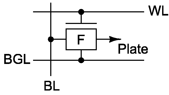
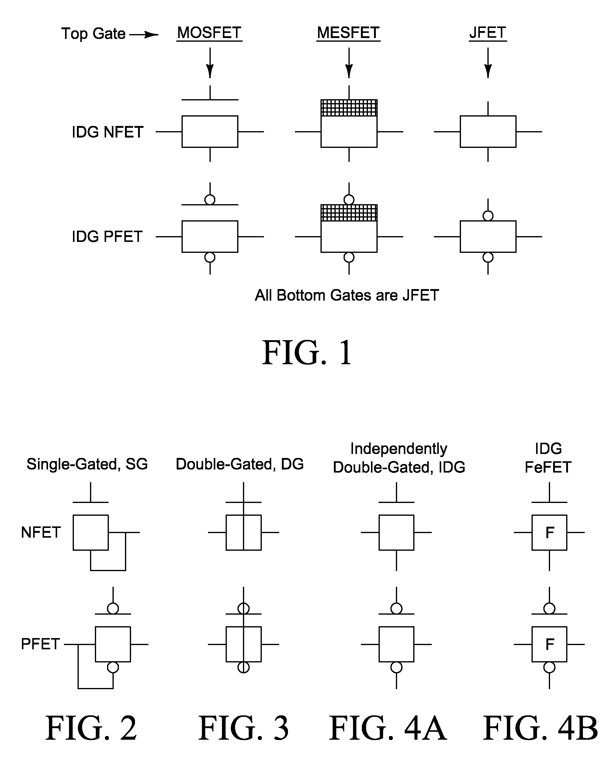
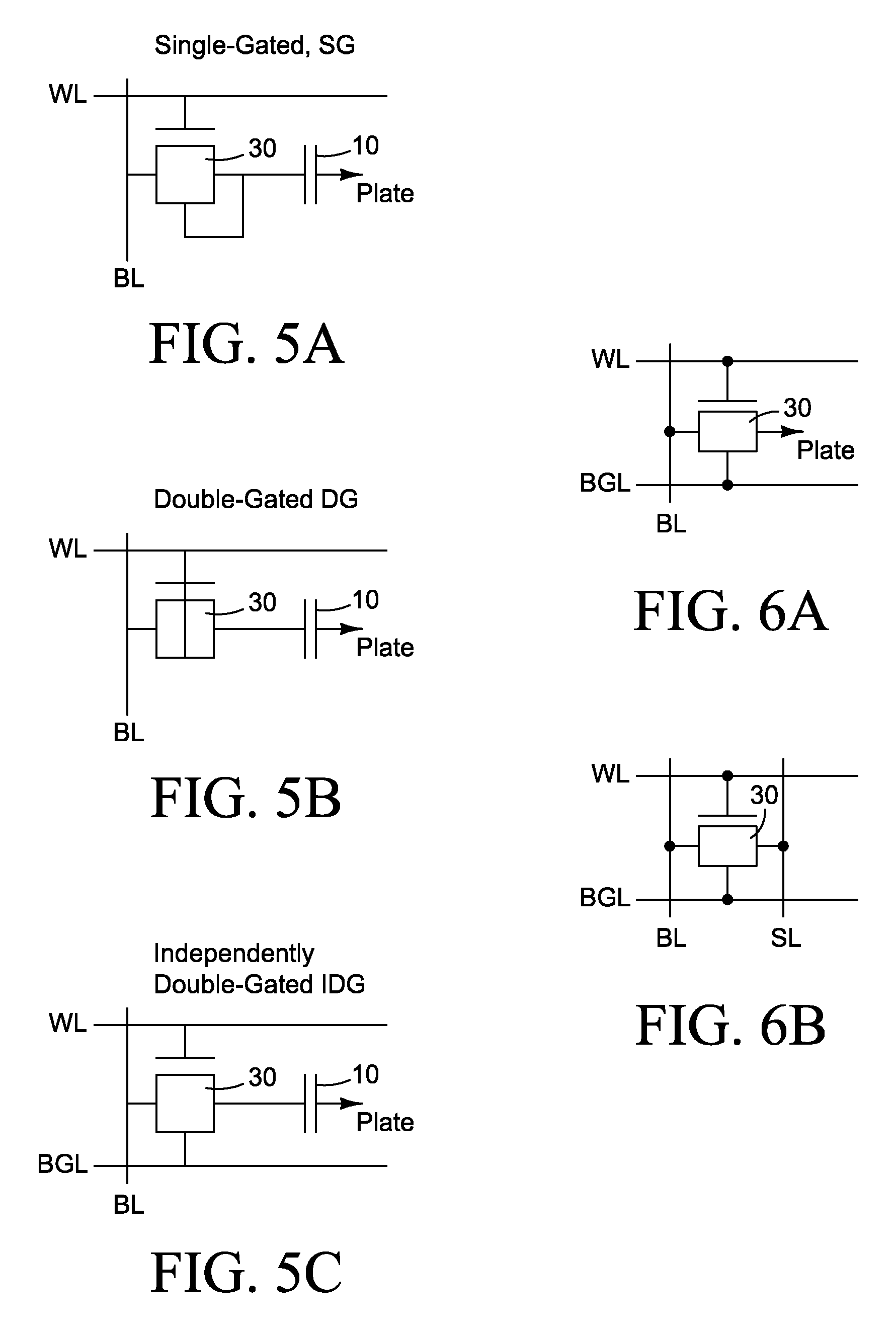
[0013]The present invention applies a double-gated CMOS Field Effect Transistor (FET) technology to the improvement of existing volatile and non-volatile (NV) Random Access Memories (RAMs), and to the realization of novel RAMs that utilize the second gate, all known existing memories being single gated. It also applies to the use of this double-gated transistor with an incorporated hysteresis-producing material, such as a ferroelectric gate insulator for a FeFET, to make possible a non-volatile, fast read / write, compact one-transistor RAM cell. The novel feature of the presently described devices is the availability of a second (bottom) gate for each transistor in the memory cell, where the second gate may be connected either independently or in parallel with the first gate. The innovation includes not just the presence of the second gate in each RAM transistor but more importantly the unique and novel ways in which the second gate is connected and utilized. The typical advantage will be to separate the writing and reading functions of the cell into two independent control lines and signals, wherein one line, separate from the other, is connected to a different terminal of the access transistor. This separation of control for writing and reading allows each function to be optimized independent of the other function.
[0014]Double-Gated (DG) Field Effect Transistors (FETs) having independent gate control accomplish the function of two parallel single-gated transistors with only a single double-gated transistor. Wherever these Independently-Double-Gated (IDG) FETs can be used, a transistor is effectively eliminated, thereby producing a smaller, more efficient memory device. Through utilization of IDG FETs, the described memory cells can be made smaller and more efficiently, and will be more power efficient than previous designs.
[0019]The incorporation of double gate (DG) transistors improves existing RAM products, especially Non-Volatile NVRAMs. In general, the application of DG transistors offers to both volatile and non-volatile RAMs the advantages of:

Problems solved by technology

As computer software programs become ever larger and more complex, more and more RAM is required in order to perform the desired computations.
As the size of RAM arrays has grown into and beyond megabits, designers of memory systems have been forced to focus much attention on considerations of size and power consumption.
Since this configuration has no inherent remanence, as there had been with the earlier magnetic core memories or with data bit latches, leakage currents allow charge to drain from the capacitor over time, resulting in a potential loss of the associated information.
Furthermore, when a conventional capacitor is used in the initial 1T-1C design the read out is destructive.
As higher density has been required of DRAM cells it has been difficult for memory designers to maintain the necessary storage capacitance of about 25 fF (femto-Farads) per cell.
The simplicity of the DRAM cell is offset by the complexity of the means for accessing and refreshing the cell.
Also, with ever higher densities, the storage capacitors on which the data is stored have become so small that they can be disturbed by ionizing radiation events resulting in soft errors.
However, flash memories have very slow write times, high voltage and power requirements, and reliability concerns.
Although significant progress has been made in this area, a common problem with transistors is the gate voltage control of the channel as the device decreases in size.
As the transistor size decreases, short-channel effects become more problematic and interfere with the gate voltage's ability to provide exclusive channel control.

Method used


Image

  • Independently-Double-Gated Transistor Memory (IDGM)
  • Independently-Double-Gated Transistor Memory (IDGM)
  • Independently-Double-Gated Transistor Memory (IDGM)

Examples


Embodiment Construction

[0079]A variety of RAMs using conventional single-gated transistors are available in research and / or production in both volatile and non-volatile forms. Some of the more conventional of these are Static SRAM, Dynamic DRAM, and NOR- and NAND-Flash Memories. More recent developments include Ferroelectric FeRAM, Magnetic MRAM, Ovonic Unified Memory (OUM) under development by Ovonyx, Inc., and Phase Change PCRAM. Each of these forms of RAM can be improved in various ways by the incorporation of a second gate in each transistor used in the memory cell. Additionally, this second gate may be connected in a variety of useful configurations. The present invention describes modifications to existing DRAM, Flash, and FeRAM cell circuits to incorporate a second gate.

[0080]All known existing memory cells utilize single-gated transistors. Some transistors that are called “double-gated” are in use but with the two gates simply tied together. The present invention involves the application of any In...


PUM


Abstract

Memory cells are constructed from double-gated four terminal transistors having independent gate control. DRAM cells may use one, two or three transistors. Single transistor cells are constructed either with or without a bit storage capacitor, and both NAND- and NOR-type Non-Volatile NVRAM cells, as well as Ferroelectric FeRAM cells, are described. For all cells, top gates provide conventional access while independent bottom gates provide control to optimize memory retention for given speed and power parameters as well as to accommodate hardening against radiation. In a single transistor cell without a capacitor, use of the bottom gate allows packing to a density approaching 2 F2. Using a ferroelectric material as the gate insulator produces a single-transistor FeRAM cell that overcomes the industry-wide Write Disturb problem. The memory cells are compatible with SOI logic circuitry for use as embedded RAM in SOC applications.

Description

CROSS-REFERENCES TO RELATED APPLICATIONS[0001]U.S. patent application Ser. No. 11 / 307,863 filed Feb. 25, 2006, entitled “Independently-Double-Gated Field Effect Transistor,” is incorporated here by reference.STATEMENT REGARDING FEDERALLY SPONSORED RESEARCH OR DEVELOPMENT[0002]Not Applicable.FIELD OF THE INVENTION[0003]The present invention relates to the composition and manufacture of solid-state memory devices. More specifically, both volatile and non-volatile memory cells are described, all of which use transistors with multiple, independent gate electrodes. Hysteresis-producing material, such as Ferroelectric insulators for transistor gates and capacitors, is incorporated into some embodiments.BACKGROUND OF THE INVENTION[0004]Temporary storage of information for today's computing devices is provided by Random Access Memory (RAM). As computer software programs become ever larger and more complex, more and more RAM is required in order to perform the desired computations. A necessa...

Claims


Application Information

Patent Timeline
Patent Type & Authority Applications(United States)
IPC IPC(8): H01L27/108H10B12/00H10B69/00
CPCG11C11/22H01L27/1203H01L27/11585G11C11/223H10B51/00
Inventor WILSON, DALE G.DEGREGORIO, KELLY J.PARKE, STEPHEN A.HACKLER, DOUGLAS R.
Owner AMERICAN SEMICON
Learn More