
Memory Element and Semiconductor Device, and Method for Manufacturing the Same

Inactive Publication Date: 2008-08-28
ORACLE INT CORP +1
View PDF75 Cites 11 Cited by
  • Summary
  • Abstract
  • Description
  • Claims
  • Application Information

AI Technical Summary

Benefits of technology

[0010]In the memory element described in Reference 2, a writing voltage value is high, and typical writing is performed with voltage of 100V in one second. In addition, in the memory element described in Reference 2, writing is also performed with voltage of 10V in ten seconds. Reference 2 describes that an interval between the electrodes is 5 μm or 10 μm and a thickness of the conjugated polymer or the oligomer is about 30 nm to 10 μm. A layer of the memory element in Reference 2 does not vary morphologically like crystal before and after application of voltage. As a result of variation of conductivity before and after application of voltage, the layer is not damaged. Reference 2 describes that variation of conductivity before and after application of voltage does not cause a loss of materials.
[0031]In accordance with the present invention, a manufacturing process of a memory element can be simplified. Further, a nonvolatile memory element and a semiconductor device that has the memory element are provided, in which data can be additionally written at a time besides the manufacturing time and in which forgery and the like caused by rewriting can be prevented. Furthermore, an inexpensive semiconductor device is provided.

Problems solved by technology

A mask ROM has a simple structure; however, it is necessary to write data during manufacturing steps thereof, and data cannot be additionally written.
An EPROM, an EEPROM, and a flash memory are nonvolatile memory circuits, and an element having two gate electrodes is used therein: therefore, there are problems in that the number of manufacturing steps thereof is increased.
A forming method of the electrode is limited due to this limitation of temperature, and an expected electrode cannot be formed.
Therefore, there are problems in that miniaturization of an element is inhibited.
A problem caused by an electrode formed over an organic layer is required to be solved from an aspect of inhibition of element miniaturization.
Therefore, there is a problem in that a manufacturing process becomes complicated.
The complicated manufacturing process is a problem that is required to be solved from an aspect of a manufacturing cost.

Method used


Image

  • Memory Element and Semiconductor Device, and Method for Manufacturing the Same
  • Memory Element and Semiconductor Device, and Method for Manufacturing the Same
  • Memory Element and Semiconductor Device, and Method for Manufacturing the Same

Examples


embodiment mode 1

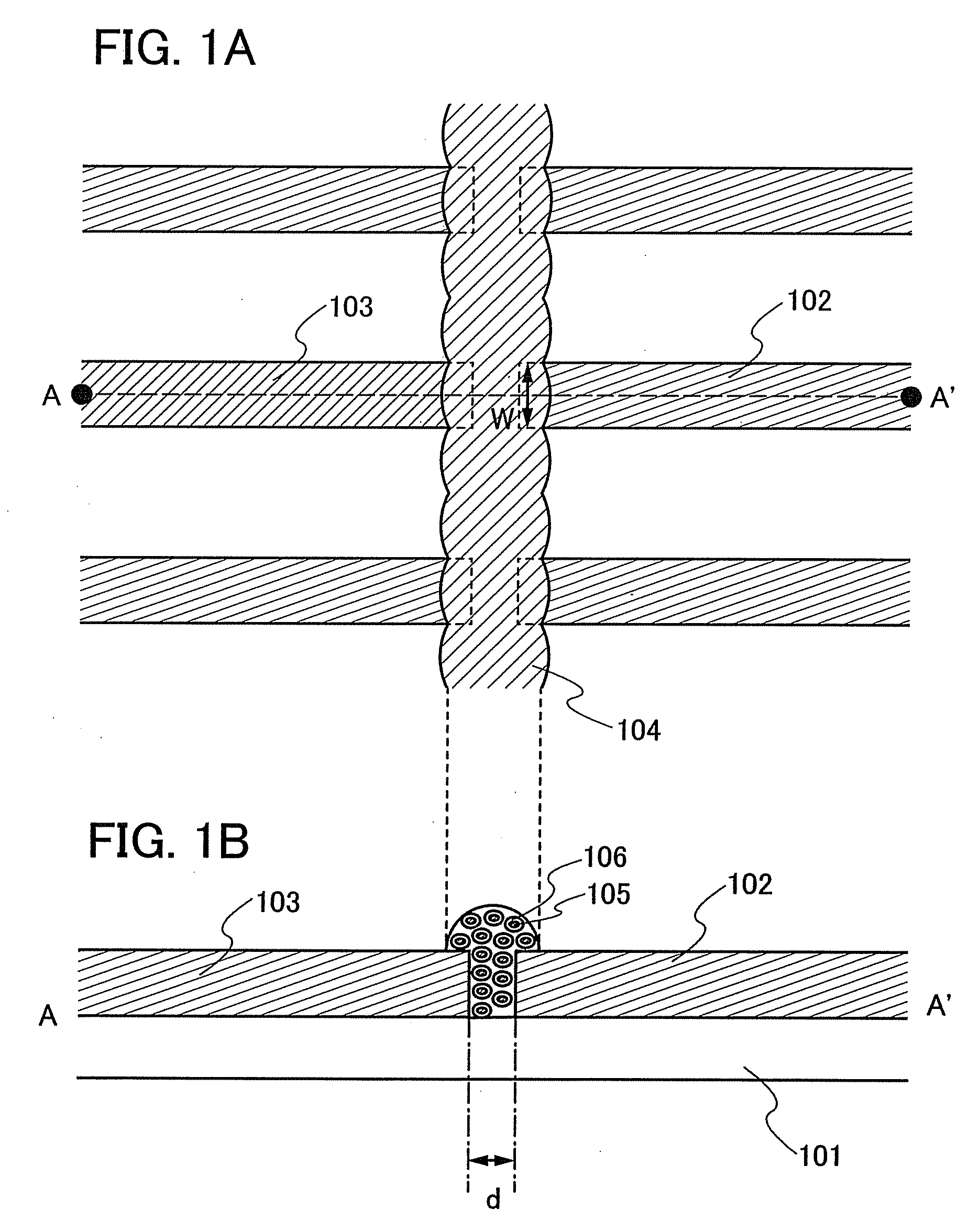
[0045]Here, an example of a semiconductor device is shown. FIG. 1A shows a top view. FIG. 1B shows a cross-sectional view taken along a line A-A′ of FIG. 1A.

[0046]In FIG. 1A, three memory elements are illustrated. Although an example of three memory elements is given here to make description simple, the number of memory elements is not particularly limited, and designers of a semiconductor device may set the number of memory elements corresponding to the desired bit number. For example, memory elements may be formed corresponding to 8 bits, 16 bits, 32 bits, 64 bits, and the like. The memory element has a structure in which a first conductive layer 102, a second conductive layer 103, and a layer 104 containing conductive fine particles deposited therebetween over a substrate 101 having an insulating surface are included as shown in FIG. 1B.

[0047]FIG. 1A shows an example in which a linear pattern of the layer 104 containing conductive fine particles is obtained by dropping of plural ...

embodiment mode 2

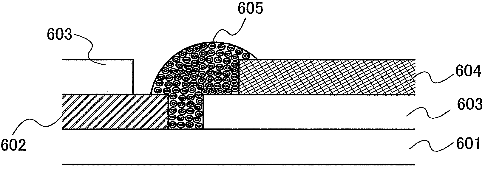
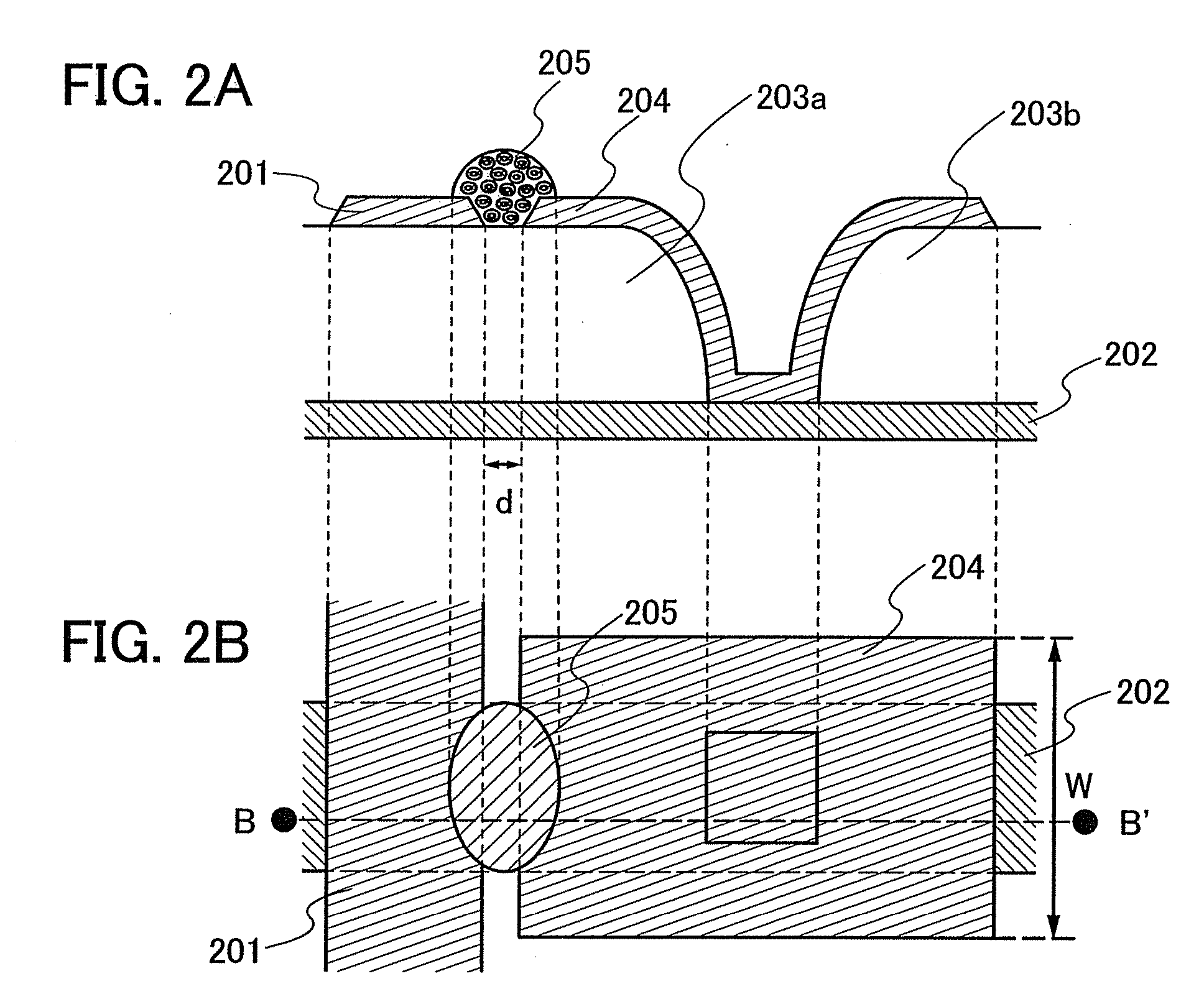
[0056]Here, a semiconductor device including a passive-matrix memory element is shown. The passive-matrix memory element is provided in the vicinity of an intersection portion of a bit line and a word line. FIG. 2B shows a top view, and FIG. 2A shows a cross-sectional view taken along a line B-B′ of FIG. 2B.

[0057]In FIG. 2A, a word line 202 is provided over a substrate having an insulating surface, and first insulating layers 203a and 203b are provided over the word line 202. The first insulating layers 203a and 203b each have a thickness of 0.8 to 1.5 μm in the vertical direction to the substrate surface. As the substrate having an insulating surface, a glass substrate, a quartz substrate, or a plastic substrate is used. As another substrate that can be used, a semiconductor substrate, an SOI substrate, a ceramic substrate, a metal substrate having an insulating film on its surface, or the like can be used.

[0058]The first insulating layers 203a and 203b are formed of the same mater...

embodiment mode 3

[0072]Here, an example of an active-matrix semiconductor device is shown. FIG. 3B shows a top view. FIG. 3A shows a cross-sectional view taken along a line C-C′ of FIG. 3B.

[0073]In FIG. 3A, a first insulating layer 302 is provided over a substrate 301 having an insulating surface, and a semiconductor layer 303 is provided thereovel A second insulating layer 304 is provided over the first insulating layer 302 and the semiconductor layer 303, and a word line (gate line) 305 is provided over the second insulating layer 304. A third insulating layer 306 is provided over the word line (gate line) 305, and a fourth insulating layer 307 is provided thereovel A bit line 309, a first electrode 308, and a common electrode 312 are provided over the fourth insulating layer 307. The bit line 309, the first electrode 308, and the common electrode 312 are formed of a same material. Six openings (contact holes) in total, which are pairs of right and left and reach the semiconductor layer 303, are p...


PUM


Abstract

It is an object to solve inhibition of miniaturization of an element and complexity of a manufacturing process thereof. It is another object to provide a nonvolatile memory device and a semiconductor device having the memory device, in which data can be additionally written at a time besides the manufacturing time and in which forgery caused by rewriting of data can be prevented. It is further another object to provide an inexpensive nonvolatile memory device and semiconductor device. A memory element is manufactured in which a first conductive layer, a second conductive layer that is beside the first conductive layer, and conductive fine particles of each surface which is covered with an organic film are deposited over an insulating film. The conductive fine particles are deposited between the first conductive layer and the second conductive layer.

Description

BACKGROUND OF THE INVENTION[0001]1. Field of the Invention[0002]The present invention relates to a semiconductor device that has a circuit including a memory element and a method for manufacturing the semiconductor device.[0003]Note that a semiconductor device in this specification refers to all types of devices which can function by utilizing semiconductor characteristics, and electro-optic devices, semiconductor circuits, and electronic devices are all included in the semiconductor device.[0004]2. Description of the Related Art[0005]A memory element using an organic compound generally has a structure in which two electrodes are provided above and below an organic compound layer, as two terminals of the memory element as described in Reference 1: United State Patent Application Laid-Open 2005 / 6640.[0006]In Reference 2: Japanese Translation of PCT International Application No. H11-504749, a memory element is proposed, having a structure in which a pair of electrodes is formed over a...

Claims


Application Information

Patent Timeline
IPC IPC(8): G11C11/34H01L21/441
CPCB82Y10/00G11C13/0002H01L2924/0002G11C13/0014G11C2213/77G11C2213/79H01L23/5252H01L27/101H01L27/105H01L27/112H01L27/11206H01L27/12H01L45/1608H01L2924/00H10B20/00H10B20/20H10N70/021
Inventor HIRAKATA, YOSHIHARU
Owner ORACLE INT CORP
Features
  • Generate Ideas
  • Intellectual Property
  • Life Sciences
  • Materials
  • Tech Scout
  • Unparalleled Data Quality
  • Higher Quality Content
  • 60% Fewer Hallucinations
Learn More