

Nano-particle light emitting material, electric field light emitting diode and ink composition each using the material, and display apparatus
- Summary
- Abstract
- Description
- Claims
- Application Information
AI Technical Summary
Benefits of technology
Problems solved by technology
Method used
Image

Examples
example 1
Synthesis of Nano-Particle Light Emitting Material
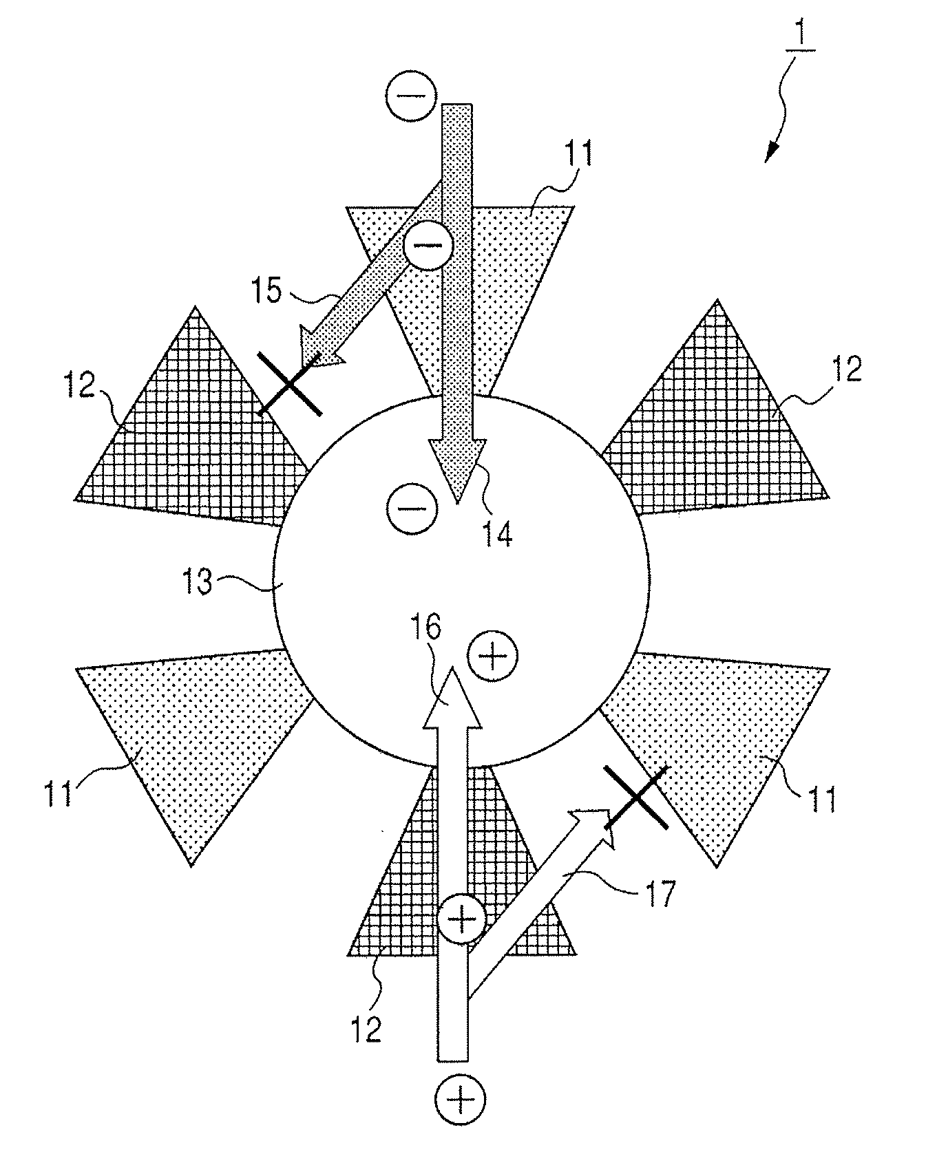
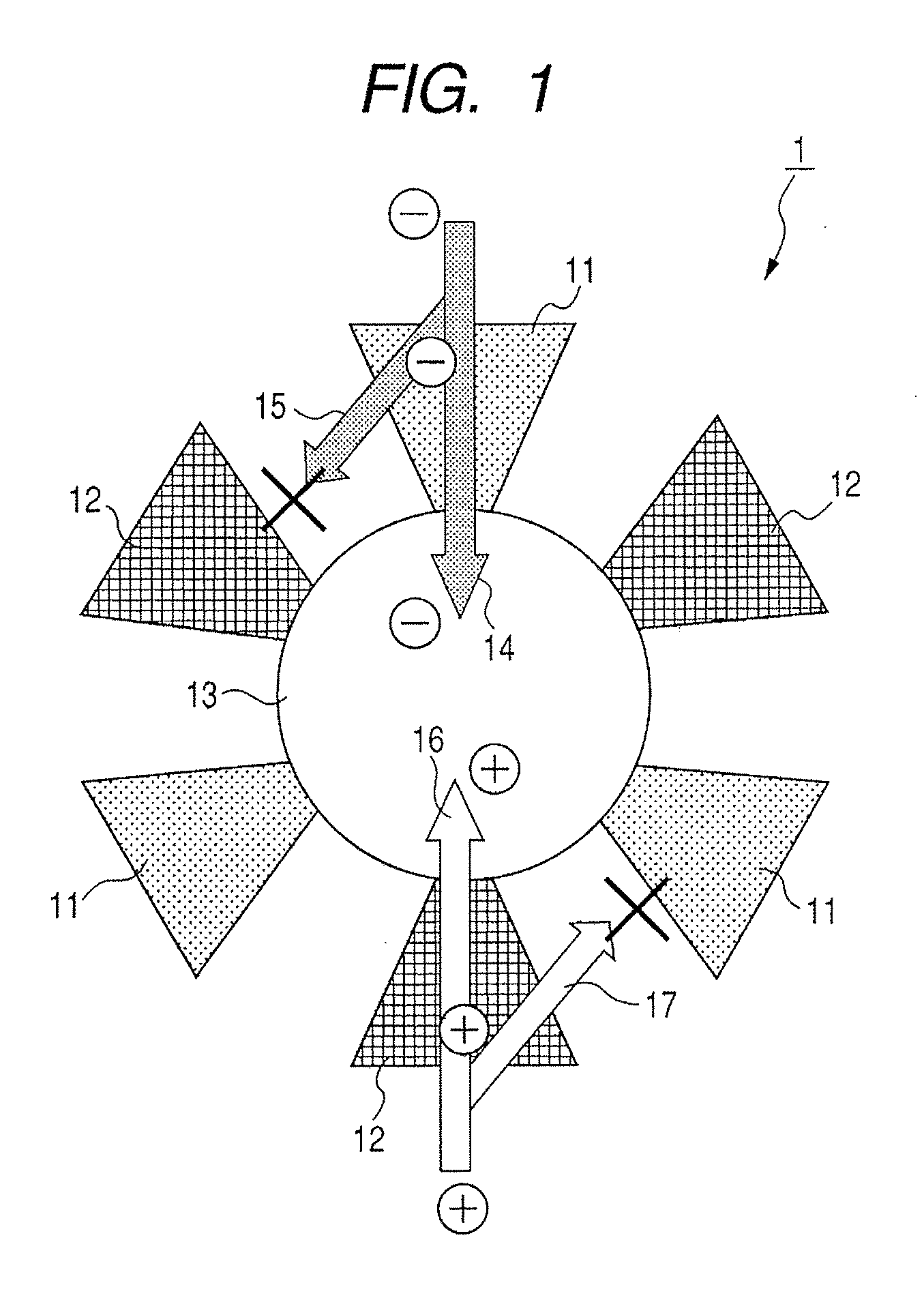
[0091]1 ml of methanol was added to 1 ml of a dispersion of CdSe nano-particles each having a surface coated with TOPO (manufactured by Evident Technologies, Inc., average core particle diameter about 4 nm, nano-particle concentration 10 mg / ml) in toluene, and the mixture was stirred. Next, the mixture was centrifuged at 12,000 rpm for 15 minutes, whereby a precipitate was produced. Next, the supernatant was removed, and the precipitated CdSe nano-particles were dried. After that, 1 ml of chloroform was added to the nano-particles, whereby a solution of the CdSe nano-particles in chloroform was obtained.
[0092]Next, 6 mg of an α-NPD derivative represented by the following formula and serving as a hole transportable ligand, and 4 mg of BPhen serving as an electron transportable ligand were added to the solution, and the mixture was stirred under a nitrogen atmosphere at room temperature for 12 hours while light was shielded so that a l...
example 2
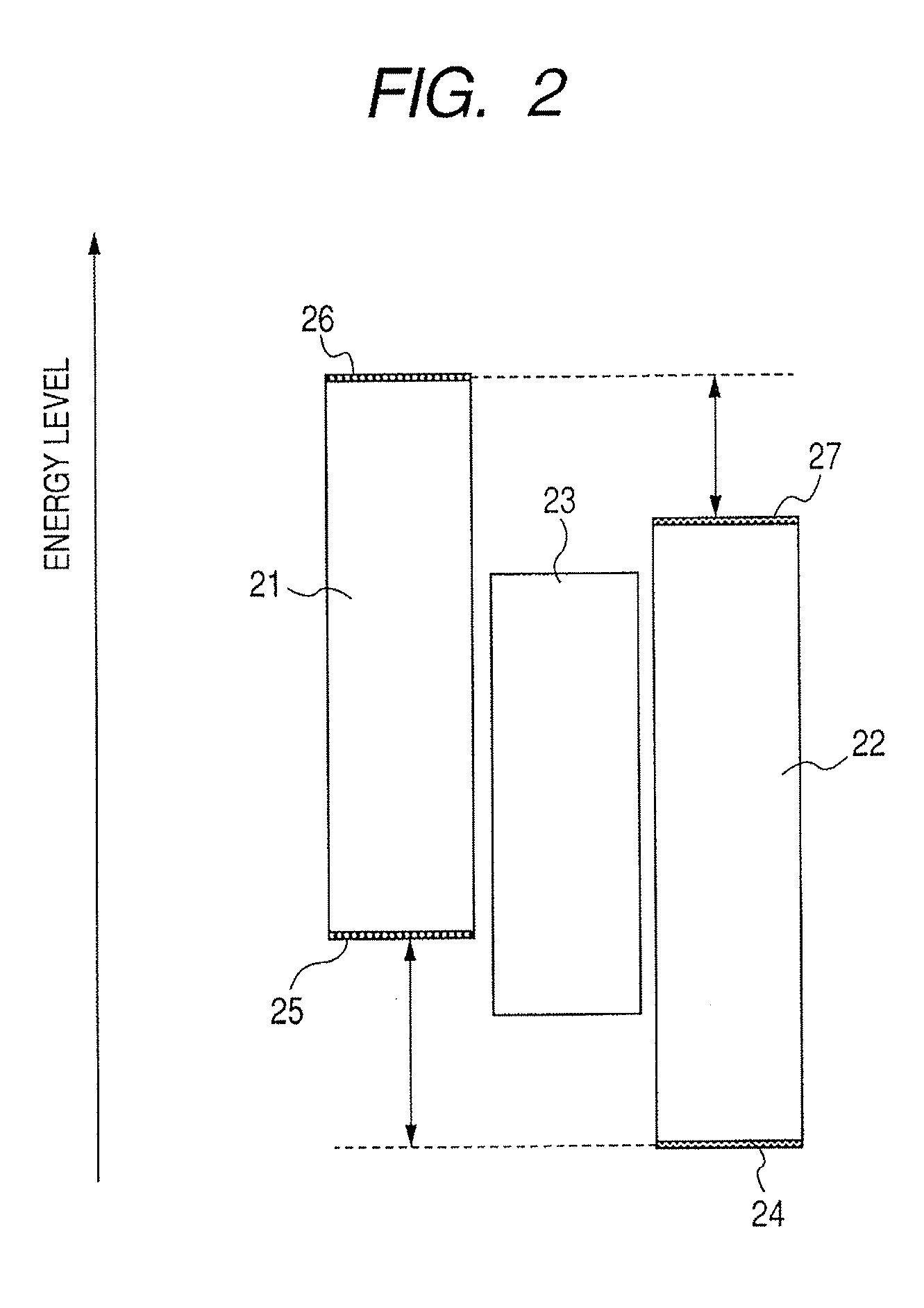
[0094]Nano-particle light emitting materials were synthesized under the same conditions as those of Example 1 except that the electron transportable ligand in Example 1 was changed to BCP. In this case, BCP had a HOMO level of −6.7 eV and a LUMO level of −3.0 eV. In addition, each CdSe nano-particle had a highest electron level in its valence band of −6.5 eV and a lowest electron level in its conduction band of −4.4 eV. Accordingly, the charge transportable ligands on the surfaces of the nano-particles of this example satisfied the conditions shown in FIGS. 2 and 4.
example 3
[0095]Nano-particle light emitting materials were synthesized under the same conditions as those of Example 2 except that CdSe / ZnS core-shell-structured nano-particles each having a surface coated with TOPO (manufactured by Evident Technologies, Inc., average core particle diameter about 5 nm, nano-particle concentration 10 mg / ml) were used as nano-particles in Example 2.
[0096]In this case, each CdSe / ZnS nano-particle had a highest electron level in the valence band of its core layer of −6.5 eV and a lowest electron level in the conduction band of the core layer of −4.4 eV. Meanwhile, the nano-particle had a highest electron level in the valence band of its shell layer of −7.5 eV and a lowest electron level in the conduction band of the shell layer of −3.4 eV. Accordingly, the charge transportable ligands on the surfaces of the nano-particles of this example satisfied the conditions shown in FIG. 5.
PUM
| Property | Measurement | Unit |
|---|---|---|
| Structure | aaaaa | aaaaa |
| Efficiency | aaaaa | aaaaa |
| Electric properties | aaaaa | aaaaa |
Abstract
Description
Claims
Application Information