

Semiconductor Manufacturing Apparatus, Method of Detecting Abnormality, Identifying Cause of Abnormality, or Predicting Abnormality in the Semiconductor Manufacturing Apparatus, and Storage Medium Storing Computer Program for Performing the Method
- Summary
- Abstract
- Description
- Claims
- Application Information
AI Technical Summary
Benefits of technology
Problems solved by technology
Method used
Image

Examples
first embodiment
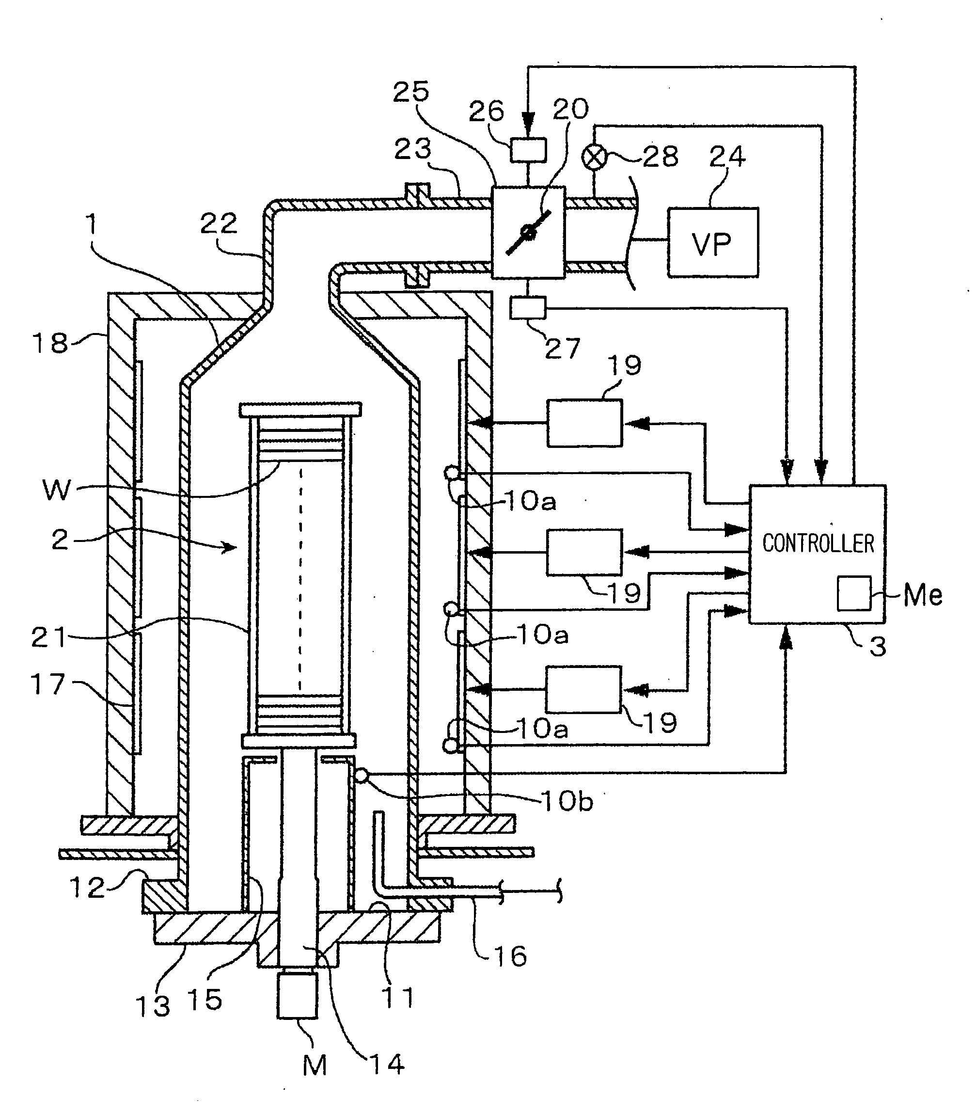
[0046]First, the overall configuration of a semiconductor manufacturing apparatus according to the present invention will be explained below referring to a vertical low-pressure CVD apparatus (deposition apparatus) which is a batch-type thermal processing apparatus as an example. In FIG. 1, a reference numeral 1 denotes a cylindrical vertical reaction vessel made of quartz. The bottom of the reaction vessel 1 is opened as a furnace throat. A flange 12 is formed around a lower end opening 11 of the reaction vessel 1. Provided at the bottom of the reaction vessel 1 is a lid 13 made of quartz, which is to be brought into contact with the underside of the flange 12 to air-tightly close the opening 11. The lid 13 is movable vertically by means of a boat elevator (elevating mechanism), not shown. A revolving shaft 14 penetrates through the center of the lid 13. A wafer boat 2 (substrate holder) is mounted on the top of the revolving shaft 14. The wafer boat 2 can be moved vertically betwe...
second embodiment
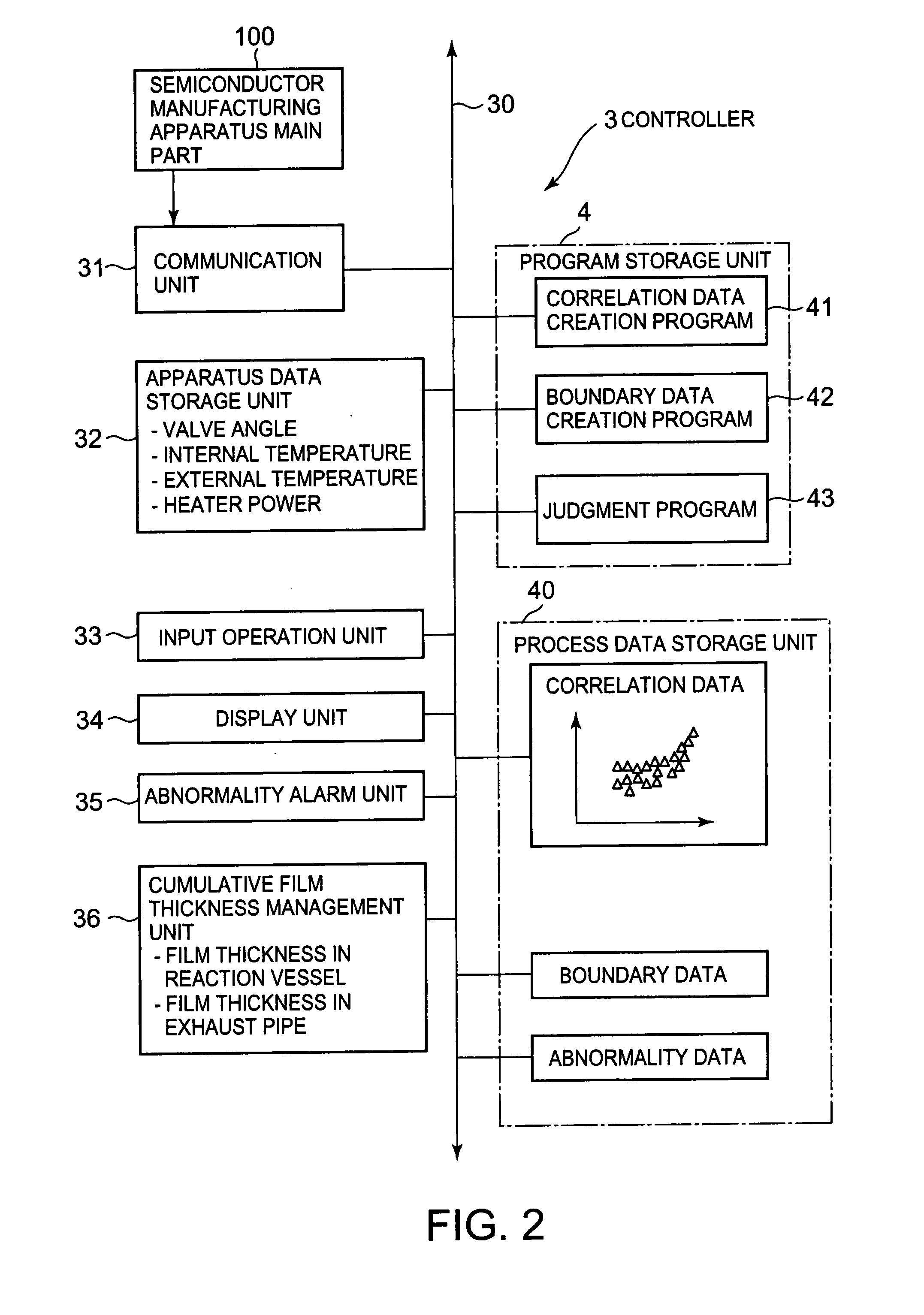
[0088]A second embodiment will be described below with reference to FIGS. 7 to 10. Each embodiment described below in the present specification differs from the first embodiment mainly in the configuration and function of the controller, but the configuration of the main part 100 of semiconductor manufacturing apparatus is the same.
[0089]In the second embodiment, the vertical low-pressure CVD apparatus is configured so that the batch size (the number of wafers or substrates which can collectively be processed) can be selected. Specifically, it is possible to collectively process not only the maximum number of wafers W which can be loaded on the wafer boat 21 but also less number of wafers. The difference in the function is realized by modifying the controller 3 without modifying the configuration of the main part 100 of semiconductor manufacturing apparatus.
[0090]The deposition apparatus according to the second embodiment can treat wafers W in three different batch sizes. FIG. 7 sch...
third embodiment
[0097]Next, a third embodiment will be described below with reference to FIGS. 11 to 18.
[0098]First, a controller 3B in the third embodiment will be described below with reference to FIG. 11, focusing on the difference from the controller 3 in the first embodiment.
[0099]Although the input operation unit 33 in the third embodiment is provided with almost the same functions as the input operation unit 33 in the first embodiment, it also plays a role of inputting various commands, such as a data search (retrieval) command (described later) when an abnormality occurs.
[0100]A program storage unit 4A in the third embodiment includes an abnormality detection program 41A, an abnormality data creation program 42A, a search (cause estimation) program 43A, and a pattern registration program 44A.
[0101]The abnormality detection program (abnormality detection means) 41A detects an abnormality of apparatus based on values of monitoring parameters (for example, internal temperature and valve angle)...
PUM
| Property | Measurement | Unit |
|---|---|---|
| Temperature | aaaaa | aaaaa |
| Thickness | aaaaa | aaaaa |
| Size | aaaaa | aaaaa |
Abstract
Description
Claims
Application Information