
Photoresist composition, coating method thereof, method of forming organic film pattern using the same and display device fabricated thereby

a technology of photoresist composition and composition, which is applied in the direction of printing, electrography/magnetography, and metallic material coating processes, etc., can solve the problems of insufficient coating of conventional photoresist composition onto large substrates with the required coating uniformity, and the inability to coat conventional photoresist composition onto large substrates by spin coating, etc., to achieve the effect of improving the coating uniformity, improving the quality of the final product, and increasing the coating rate of the photoresist composition

Inactive Publication Date: 2008-09-04
SAMSUNG DISPLAY CO LTD
View PDF8 Cites 16 Cited by
  • Summary
  • Abstract
  • Description
  • Claims
  • Application Information

AI Technical Summary

Benefits of technology

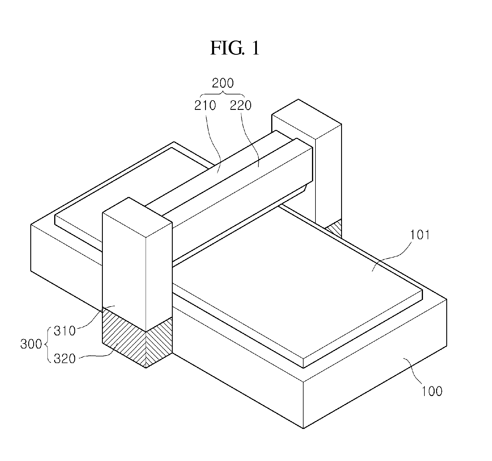
[0013]Therefore, in view of the limitations of the prior art, provided herein is a photoresist composition for coating onto a large substrate, having improved coating uniformity, which prevents the occurrence of stains such as resin streaks and cumulous stains, and which increases the coating rate of a photoresist composition on a surface of a substrate when using a spinless coating method, and thereby improves the quality of a final product prepared therefrom; a coating method for the photoresist composition; a method of forming an organic film pattern using the photoresist composition; and a display device fabricated with the photoresist composition.
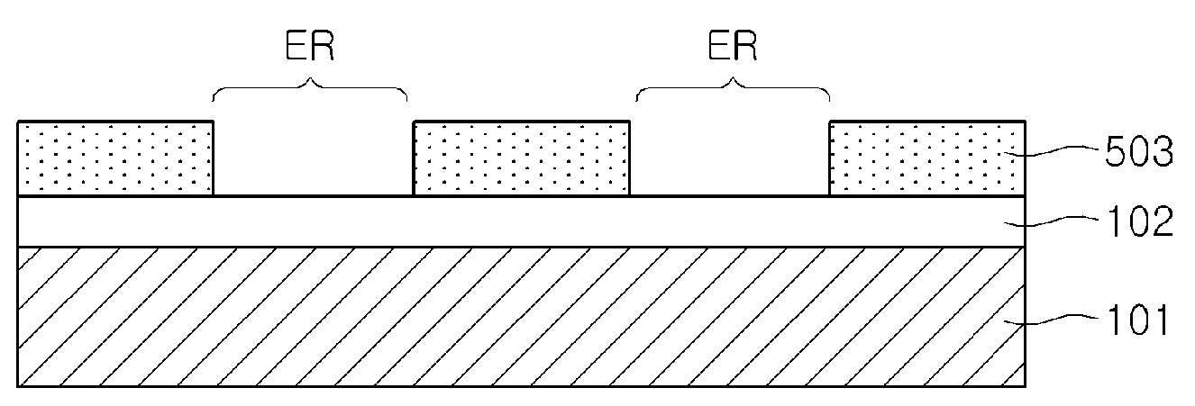
[0036]In an embodiment, patterning the photoresist composition comprises drying the photoresist composition under reduced pressure, soft baking the dried photoresist composition, selectively exposing the soft baked photoresist composition to light, developing the selectively exposed photoresist composition, and curing the developed photoresist composition.

Problems solved by technology

Recently, as the demand for large LCDs increase, a commensurate increase in the size of the substrate for such LCDs is inevitably required.
Furthermore, when fabricating a large LCD, conventional photoresist composition coating methods such as roll coating, spin coating, slit and spin coating, or the like, are not sufficient to coat a photoresist composition onto a large substrate with the required coating uniformity.
In particular, it is impossible to coat a conventional photoresist composition onto a large substrate by spin coating, as the durability of a spin motor for a spin coating apparatus that would ordinarily be used would be insufficient given the size of the substrate.
However, the slit nozzle coating device causes resin streaks, and also produces cumulous stains, neither of which is generated by the conventional spin coating process.
The cumulous stain may be created over a portion of the substrate, or the entire area of the substrate, and is mainly caused by non-uniformity of the coating thickness.
The presence of streaks and / or stains increases the defect ratio for the entire process and reduces the quality of the final product.
However, conventional polyacrylate based resin materials are limited as to either or both of high transmissivity and sensitivity.

Method used


Image

  • Photoresist composition, coating method thereof, method of forming organic film pattern using the same and display device fabricated thereby
  • Photoresist composition, coating method thereof, method of forming organic film pattern using the same and display device fabricated thereby
  • Photoresist composition, coating method thereof, method of forming organic film pattern using the same and display device fabricated thereby

Examples


experimental example 1

[0129]A photoresist composition for a liquid crystal display device circuit was prepared by mixing 82 g of a mixture of DAA, PGME and ACAC in a weight ratio of 45:25:30 respectively (i.e., 36.9 g of DAA, 20.5 g of PGME and 24.6 g of ACAC) as the organic solvent with 1.0 g of a photosensitizer and 17.0 g of a polysiloxane resin(silicone resin; SF-P2020 from TORAY) and then agitating the mixture to a rotating speed of 40 rpm at room temperature.

[0130]The photosensitizer was a mixture of 2,3,4-trihydroxy benzophenone-1,2-naphthoquinonediazide-5-sulfonate and 2,3,4,4′-tetrahydroxybenzophenone-1,2-naphthoquinonediazide-5-sulfonate, mixed at a weight ratio of 1:1 (i.e., 0.5 g of each compound), and 500˜4000 ppm. of an F-based surfactant was also included.

[0131]The resulting photoresist composition had a viscosity of 4.7 cps and within the recommended range of viscosity for use with a slit coater.

[0132]The prepared photoresist composition for a liquid crystal display device circuit was coa...

experimental example 2

[0133]A photoresist composition for a liquid crystal display device circuit was prepared in the same method as in the experimental example 1, except that a mixture of DAA and PGME, mixed in a weight ratio of 70:30 respectively (i.e., 57.4 g of DAA and 24.6 g of PGME) was used as the organic solvent.

experimental example 3

[0134]A photoresist composition for a liquid crystal display device circuit was prepared by the same method as that used in the Experimental Example 1, except that DAA and CP mixed at a weight ratio of 65:35 (i.e., 53.3 g of DAA and 28.7 g of CP) were used as the organic solvents.


PUM

PropertyMeasurementUnit
viscosityaaaaaaaaaa
sizeaaaaaaaaaa
pressureaaaaaaaaaa

Abstract

Disclosed herein is a photoresist composition suitable for coating onto a large substrate and having improved coating uniformity to prevent occurrence of stains, a coating method thereof, a method of forming an organic film pattern using the same, and a display device fabricated thereby. The present invention thus provides a photoresist composition comprising a polymeric resin with an incorporated polysiloxane resin, a photosensitive compound, and an organic solvent. Accordingly, the photoresist composition can be coated onto a large substrate by a spinless coating method, and thereby coating uniformity can be improved, the occurrence of stains such as cumulous stains and resin streaks can be prevented, and the coating rate and quality of a final product prepared using the photoresist composition can also thereby be enhanced.

Description

[0001]This application claims priority to Korean Patent Application No. 10-2007-0011271 filed on Feb. 2, 2007, and all the benefits accruing therefrom under 35 U.S.C. 119(a), the content of which is disclosed herein by reference in its entirety.BACKGROUND OF THE INVENTION[0002]1. Field of the Invention[0003]The present invention relates to a photoresist composition, a coating method thereof, a method of forming an organic film pattern using the same, and a display device fabricated thereby, and more particularly, to a photoresist composition for coating onto a large substrate with improved coating uniformity to prevent occurrence of stains, a coating method thereof, a method for forming an organic film pattern using the same, and a display device fabricated thereby.[0004]2. Description of the Related Art[0005]A liquid crystal display (“LCD”) is one of various types of flat panel display that are currently and widely used. An LCD is configured by arranging a thin film transistor subs...

Claims


Application Information

Patent Timeline
Patent Type & Authority Applications(United States)
IPC IPC(8): G03F7/004B05D1/02G03F7/20
CPCG03F7/0233Y10T428/24802G03F7/40G03F7/0757G03F7/0045
Inventor LEE, YEONG BEOMKIM, KYUNG SEOPLEE, JUN YOUNGKANG, SUNG WOOK
Owner SAMSUNG DISPLAY CO LTD
Learn More