Isolated Bipolar Transistor

a bipolar transistor and transistor technology, applied in the direction of basic electric elements, semiconductor devices, electrical equipment, etc., can solve the problems of not facilitating complete electrical isolation, unable to facilitate the electrical isolation of its fabricated devices, and unable to facilitate competitive electrical isolation

Inactive Publication Date: 2008-09-11
ADVANCED ANALOGIC TECHNOLOGIES INCORPORATED
View PDF88 Cites 76 Cited by
  • Summary
  • Abstract
  • Description
  • Claims
  • Application Information

AI Technical Summary

Benefits of technology

[0014]Isolated CMOS transistors of this invention are formed in an isolated pocket of the substrate, which is bounded by a floor isolation region of opposite conductivity type to the substrate and a filled trench extending downward from the surface of the substrate at least to the floor isolation region. The filled trench comprises a dielectric material and may be completely filled with the dielectric material or may have walls lined with the dielectric material and include a conductive material extending from the surface of the substrate to the floor isolation region. The substrate does not include an epitaxial layer, avoiding the many problems described above.

Problems solved by technology

While both LOCOS and trench isolation can prevent unwanted surface conduction between devices, they do not facilitate complete electrical isolation.
Although conventional CMOS wafer fabrication offers high density transistor integration, it does not facilitate compete electrical isolation of its fabricated devices.
This restriction is substantial, preventing the use of the NMOS as a high-side switch, an analog pass transistor, or as a bidirectional switch.
It also makes current sensing more difficult and often precludes the use of integral source-body shorts needed to make the NMOS more avalanche rugged.
Moreover since the P-type substrate in a conventional CMOS is normally biased to the most negative on-chip potential (defined as “ground”), every NMOS is necessarily subjected to unwanted substrate noise.
While not as ideal as dielectric isolation, where oxide surrounds each device or circuit, junction isolation has historically offered the best compromise between manufacturing cost and isolation performance.
Growth of epitaxial layers is slow and time consuming, representing the single most expensive step in semiconductor wafer fabrication.
The isolation diffusion is also expensive, performed using high temperature diffusion for extended durations (up to 18 hours).
Prior to epitaxial growth however, this NBL layer must be diffused sufficiently deep to reduce its surface concentration, or otherwise the concentration control of the epitaxial growth will be adversely impacted.
Because the NBL is comprised of a slow diffuser, this pre-epitaxy diffusion process can take more than ten hours.
Only after isolation is complete, can conventional CMOS fabrication commence, adding considerable time and complexity to the manufacturing of junction isolated processes compared to conventional CMOS processes.
These high temperature processes are expensive and difficult to perform, and they are incompatible with large diameter wafer manufacturing, exhibiting substantial variation in device electrical performance and preventing high transistor integration densities.
Another disadvantage of junction isolation is the area wasted by the isolation structures and otherwise not available for fabricating active transistors or circuitry.
As a further complication, with junction isolation, the design rules (and the amount of wasted area) depend on the maximum voltage of the isolated devices.
Obviously, conventional epitaxial junction isolation, despite its electrical benefits, is too area wasteful to remain a viable technology option for mixed signal and power integrated circuits.
While this “epi-less” low thermal budget technique has many advantages over non-isolated and epitaxial junction isolation processes, in some cases its reliance on LOCOS may impose certain limitations on its ability to scale to smaller dimensions and higher transistor densities.
As described, a fully-isolated BCD process with implants contoured to LOCOS, while easily implemented using a 0.35 micron based technology, may encounter problems when scaled to smaller dimensions and tighter line widths.
The narrow LOCOS bird's beak however may cause the width of the isolation sidewall to become narrowed and isolation quality may be sacrificed.

Method used


Image

  • Isolated Bipolar Transistor
  • Isolated Bipolar Transistor
  • Isolated Bipolar Transistor

Examples


Embodiment Construction

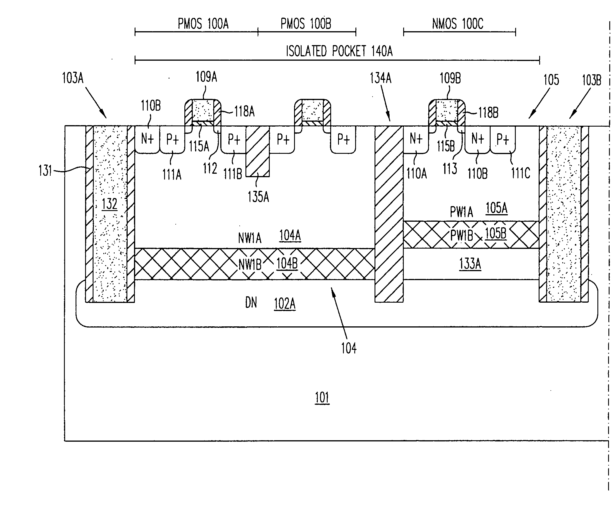
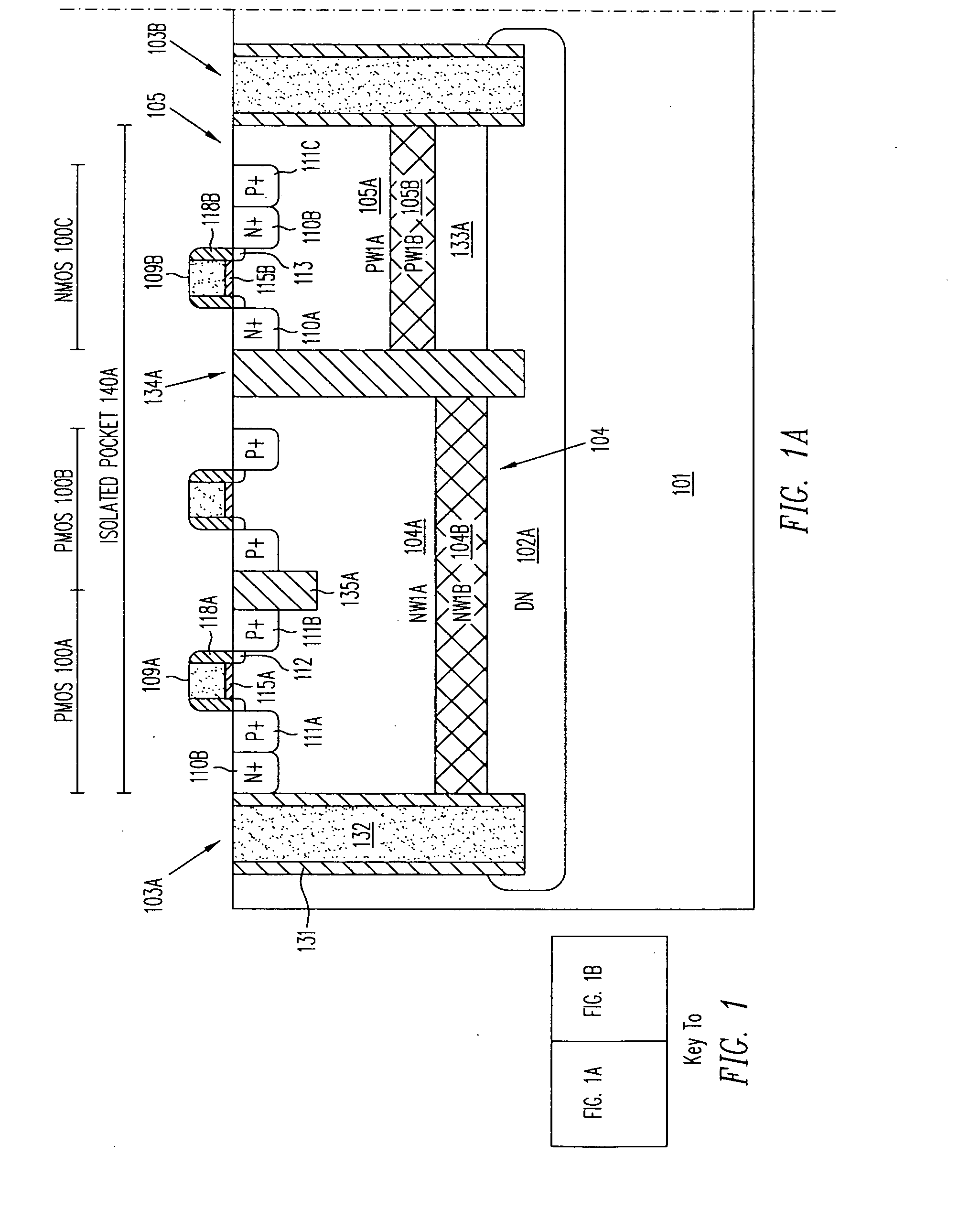
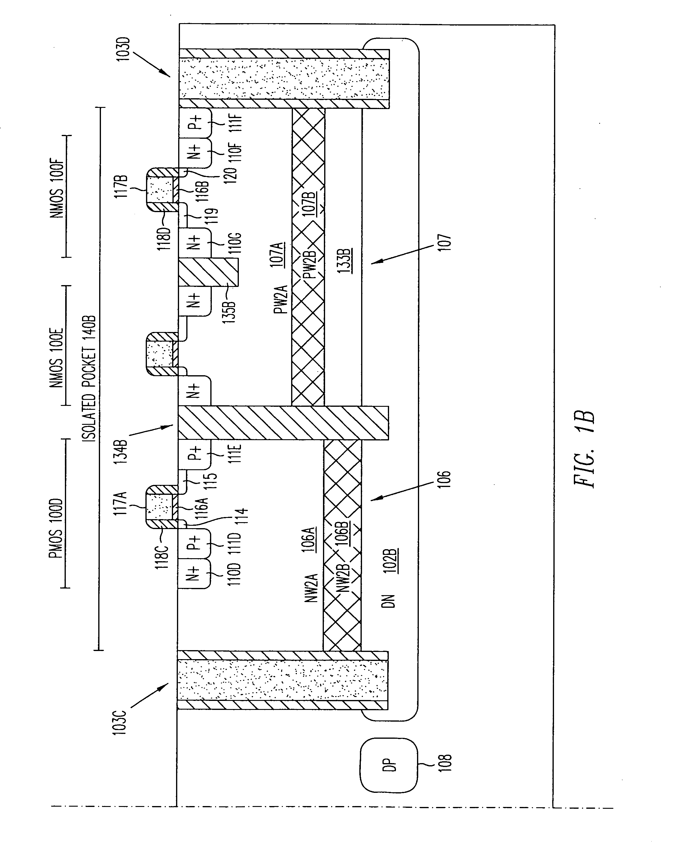
[0041]Initially, various isolated CMOS and bipolar transistors that can be fabricated in accordance with this invention will be described. This will be followed by a description of alternative process flows for fabricating the isolation structures.

[0042]FIG. 1 illustrates a cross-sectional view of isolated CMOS devices fabricated in a common P-type substrate 101. A PMOS 100A, a PMOS 100B, and an NMOS 100C are formed in a pocket 140A, which is isolated from substrate 101 by a deep implanted DN floor isolation region 102A and filled trenches 103A and 103B. The sidewalls of trenches 103A and 103B are covered with a layer 131 of dielectric material and the interior parts of the trenches are filled with a conductive material 132. The conductive material provides contact from the surface to the DN region 102A, and the dielectric material 131 insulates the conductive material 132 from the substrate 101 and from isolated pocket 140A. Trenches 103A and 103B are preferably portions of a singl...


PUM


Abstract

An isolated bipolar transistor formed in a P-type semiconductor substrate includes an N-type submerged floor isolation region and a filled trench extending downward from the surface of the substrate to the floor isolation region. Together the floor isolation region and the filled trench form an isolated pocket of the substrate which contains the bipolar transistor. The collector of the bipolar transistor may comprise the floor isolation region. The substrate does not contain an epitaxial layer, thereby overcoming the many problems associated with fabricating the same.

Description

CROSS-REFERENCE TO RELATED APPLICATIONS[0001]This application is a continuation-in-part of application Ser. No. 11 / 890,993, filed Aug. 8, 2007. application Ser. No. 11 / 890,993 is a continuation of application Ser. No. 11 / 444,102, filed May 31, 2006, and a continuation-in-part of the following applications: (a) application Ser. No. 10 / 918,316, filed Aug. 14, 2004, which is a divisional of application Ser. No. 10 / 218,668, filed Aug. 14, 2002, now U.S. Pat. No. 6,900,091, and (b) application Ser. No. 11 / 204,215, filed Aug. 15, 2005, which is a divisional of application Ser. No. 10 / 218,678, filed Aug. 14, 2002, now U.S. Pat. No. 6,943,426. Each of the foregoing applications and patents is incorporated herein by reference in its entirety.BACKGROUND OF THE INVENTION[0002]In the fabrication of semiconductor integrated circuit (IC) chips, it is frequently necessary to electrically isolate different devices from the semiconductor substrate and from each other. One method of providing lateral...

Claims


Application Information

Patent Timeline
Patent Type & Authority Applications(United States)
IPC IPC(8): H01L49/00
CPCH01L21/761H01L21/76243H01L21/76267H01L21/763H01L21/8222H01L21/82285H01L29/732H01L21/823892H01L27/0825H01L27/0826H01L29/1004H01L29/41708H01L21/823878
Inventor DISNEY, DONALD R.WILLIAMS, RICHARD K.
Owner ADVANCED ANALOGIC TECHNOLOGIES INCORPORATED
Why Eureka
Try Eureka