Optical sensor based on surface electromagnetic wave resonance in photonic band gap materials

a technology of photonic band gap and optical sensor, applied in the field of optical sensor configuration, can solve the problems of gold having a less well-defined resonance than silver, and being suitable for most applications, and having some limitations on the surface plasmon sensor

Inactive Publication Date: 2008-09-11
ROBERTSON WILLIAM M
View PDF10 Cites 26 Cited by
  • Summary
  • Abstract
  • Description
  • Claims
  • Application Information

AI Technical Summary

Benefits of technology

[0007]The present invention provides for an optical multilayer structure constructed so as to cause the structure to exhibit a photonic band gap. In one exemplary embodiment, the structure comprises an optical multilayer deposited or disposed on an optically transparent substrate or side of a prism, the optical multilayer being formed of a series of alternative ...

Problems solved by technology

In practice, surface plasmon sensors have some limitations.
However, because silver is chemically reactive it is not suitable in most applications.
However, gold has a less well-defined resonance than silver because of its higher dielectric loss.
Gold films have limited sensitivity to dielectric changes at the surface because of the difficulty of accurately detecting small angle shifts of the broad resonance.
Furthermore, the optical properties of gold me...

Method used


Image

  • Optical sensor based on surface electromagnetic wave resonance in photonic band gap materials
  • Optical sensor based on surface electromagnetic wave resonance in photonic band gap materials
  • Optical sensor based on surface electromagnetic wave resonance in photonic band gap materials

Examples


Embodiment Construction

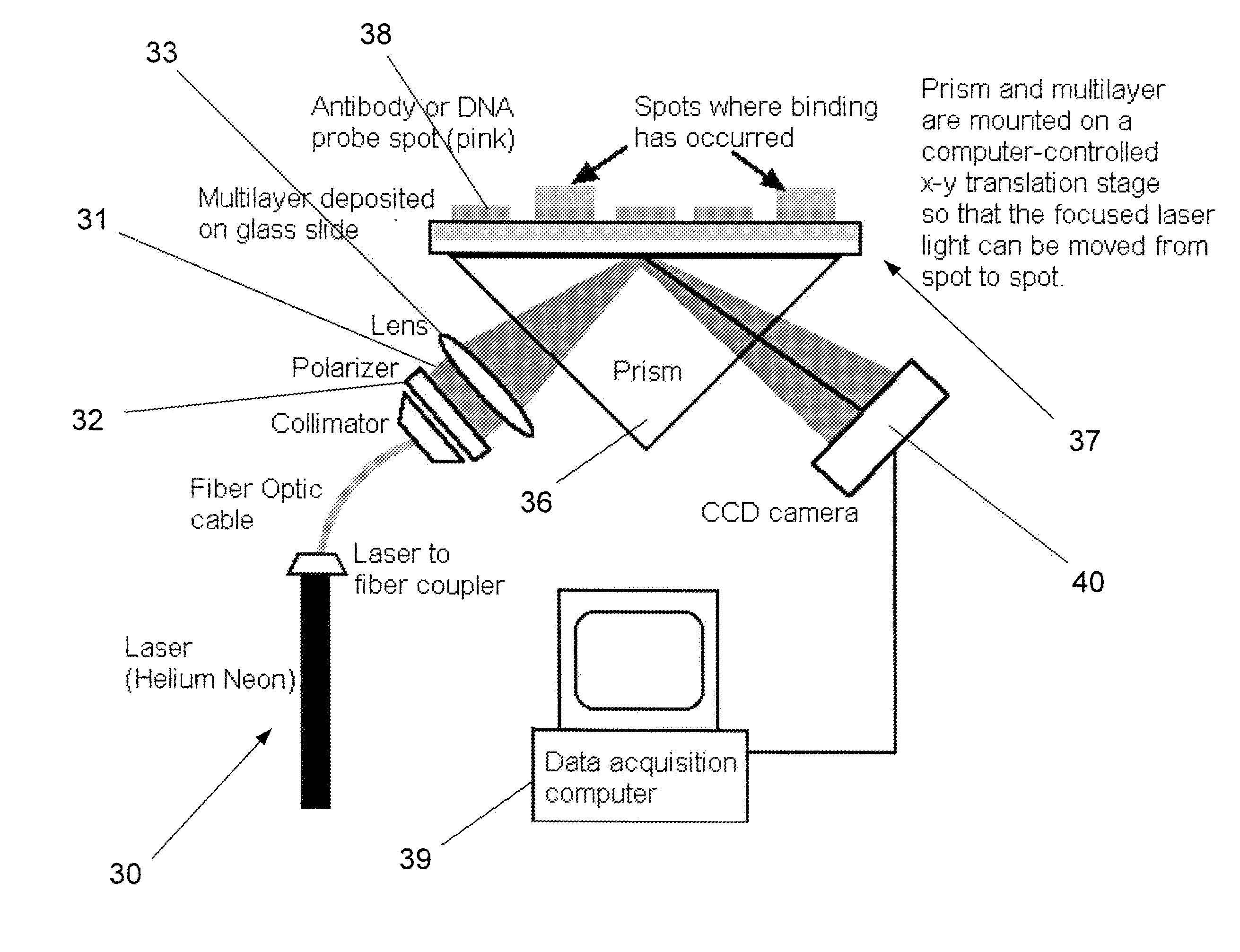
[0024]Surface electromagnetic (EM) waves are electromagnetic modes that propagate at the interface between a passive dielectric material and a so-called active medium (i.e., one whose real part of the dielectric function is less than −1 at the frequency of interest). The dispersion of surface EM waves is such that they are non-radiative, which means that they do not couple directly to light. Excitation of surface EM modes requires the use of a prism or a grating configuration in order to phase match incident light to the surface mode and facilitate resonant coupling between light and the surface EM modes.

[0025]The most widely studied type of surface electromagnetic waves are those that exist at the surfaces of metals. These modes are known as surface plasmons. A number of metals exhibit a sufficiently negative real part of the dielectric function so as to support surface plasmons; however, most metals also have strong dielectric loss (i.e., the large imaginary part of the dielectric...


PUM


Abstract

A sensing method and apparatus using photonic band gap multilayered material. Photonic band gap multi-layers are formed from alternating layers of higher refractive index and lower refractive index materials, and may be deposited or disposed on a optically transparent substrate or a reflecting face of a prism. Light is directed into the prism, directed to the photonic band gap multilayer, and reflected out of the prism, where it is captured and analyzed. Various sensor configurations keep light wavelength or coupling angle fixed, while monitoring the change in the other parameter. Also disclosed is a microarray configuration with an array of probe spots placed on one surface of the multilayer, which is mounted on an x-y translation stage. Also disclosed is a configuration where a cylindrical lens focuses an expanded and collimated light beam to a line that transects the rows of array elements sequentially, producing an image with shifted surface electromagnetic wave modes for each row, corresponding to individual elements of the array row.

Description

[0001]This application is a continuation-in-part of U.S. patent application Ser. No. 11 / 468,343, filed Aug. 30, 2006, by William M. Robertson, which claims the benefit of Provisional Patent Application No. 60 / 712,682, filed Aug. 30, 2005, by William M. Robertson, and Provisional Patent Application No. 60 / 806,210, filed Jun. 29, 2006, by William M. Robertson, and is entitled in whole or in part to those filing dates for priority. The specifications, drawings, and attachments of Provisional Patent Application Nos. 60 / 712,682 and 60 / 806,210, and U.S. patent application Ser. No. 11 / 468,343, are incorporated herein in their entirety by reference.FIELD OF INVENTION[0002]The invention disclosed herein involves optical sensing configurations designed to detect trace amounts of biological and chemical entities, as well as methods for utilizing these sensors. In particular, one embodiment of the present invention is directed towards a sensor and method of microarray analysis using surface opt...

Claims


Application Information

Patent Timeline
IPC IPC(8): G02B5/126G01N21/55G01J3/28
CPCG01N21/553G01N21/253
Inventor ROBERTSON, WILLIAM M.
Owner ROBERTSON WILLIAM M
Why Eureka
Try Eureka