

Scanning probe microscope and sample observation method using the same and device manufacturing method
a scanning probe and microscope technology, applied in the direction of measuring devices, mechanical roughness/irregularity measurements, instruments, etc., can solve the problems of distorted measurement shape, probe wear, and difficulty in the current cd-sem to deal with the above described problems and requirements, and achieve stable and accurate device manufacturing, high accuracy, and high speed
- Summary
- Abstract
- Description
- Claims
- Application Information
AI Technical Summary
Benefits of technology
Problems solved by technology
Method used
Image

Examples
embodiment 1
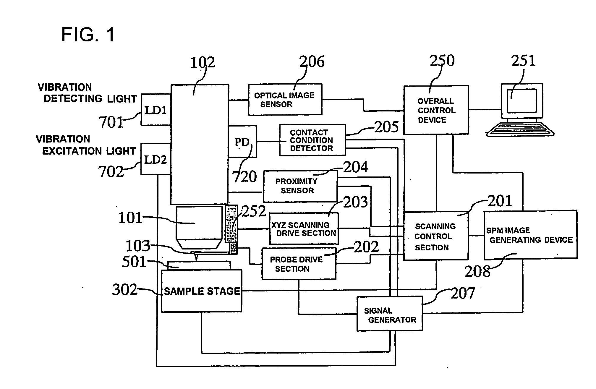
[0041]FIG. 1 shows the construction of a scanning probe microscope according to Embodiment 1 of the present invention. A sample 501 is placed on a sample stage 302 which can be driven in the X, Y, Z directions and controlled by a scanning control section 201. A probe transfer mechanism 252 provided with a probe 103 is driven in the X, Y, Z directions by a signal from a XYZ scanning drive section 203 to thereby perform probe scanning of the scanning probe microscope.
[0042]It is possible to generate minute vibration in the probe 103 itself or an actuator made up of a piezoelectric element or the like disposed at the base of the probe by a signal from a probe drive section 202. Or as another embodiment, the signal from the probe drive section 202 may be superimposed on the signal from the XYZ scanning drive section 203 to cause minute vibration in the probe transfer mechanism and thereby excite vibration in the probe 103 attached. Or as will be described later, vibration excitation lig...
embodiment 2
[0076]FIG. 6 illustrates an optical system of a scanning probe microscope according to Embodiment 2 of the present invention. Light emitted from a light source 111 is transformed to parallel light by a lens 112, reflected by a mirror 113, introduced to a lens 101 and focused on a sample 501. An image in an arbitrary shape such as a spot or slit can be formed depending on the shape of the opening incorporated in the light source 111. Light reflected on the sample passes through an objective lens again, reflected by a mirror 114 and an image thereof is formed on a detector 116 through an image forming lens 115. The position of the image is moved according to the height of the sample 501. The amount of movement is expressed by 2πZ tan θ, where θ is the angle of incidence of detection light 110 upon the sample, m is image forming magnification by the lens 115 and Z is the height of the sample, and therefore it is possible to detect the height Z of the sample by measuring this amount of ...
embodiment 3
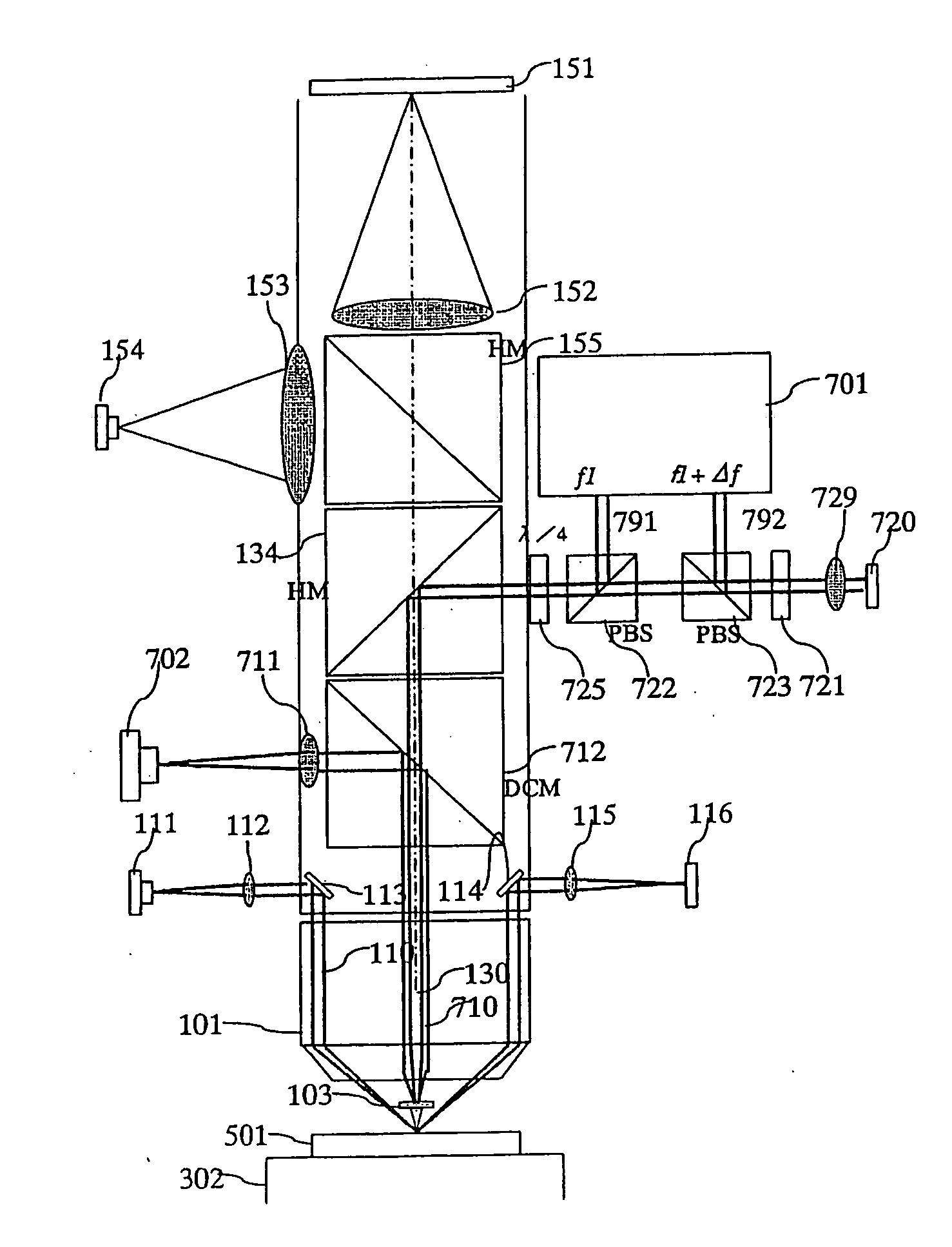
[0084]FIG. 7 shows an optical system according to Embodiment 3 of the present invention. Embodiment 2 uses so-called heterodyne detection using two-frequency light, but instead of heterodyne detection, it is also possible to use homodyne detection using light of a single frequency. In this case, this embodiment is the same in that light of frequency f1 is branched and used as reference light 792 and detected on a photodiode, but in order to detect the phase, a laser is branched by a half mirror 726 as shown in FIG. 7, one beam is reflected by a mirror 727, a phase difference of 90 degrees between the reference light and detected light is provided using a λ / 4 wave plate 728, both beams are made to interfere with each other by a polarizing plate 721′, passed through a lens 729′ and detected by a second photodiode 720′. Signals from the first and second photodiodes 720, 720′ become signals corresponding to cos and sin and by detecting the amplitudes of the components corresponding to r...
PUM
 Abstract
Description
Claims
Application Information