Flip-chip substrate

a technology of substrate and chip, which is applied in the direction of printed circuit manufacturing, printed circuit aspects, metallic pattern materials, etc., can solve the problems of reducing yield and reliability, reducing the thermal expansion coefficient of bt resin and abf resin, and preventing substrate warpage, excellent thermal and mechanical properties, and fine-patterned circuit layout

Inactive Publication Date: 2008-09-25
PHOENIX PRECISION TECH CORP
View PDF7 Cites 17 Cited by
  • Summary
  • Abstract
  • Description
  • Claims
  • Application Information

AI Technical Summary

Benefits of technology

[0012]The present invention provides a flip-chip substrate using aluminum oxide, which has excellent thermal properties and mechanical properties (for example, the Young's modulus of aluminum o

Problems solved by technology

Unfortunately, the coefficient of thermal expansion (CTE) of BT resin and ABF resin are different.
The CET difference causes substrate warpage to the flip-chip substrate such that the yield and the reliabilit

Method used


Image

  • Flip-chip substrate
  • Flip-chip substrate
  • Flip-chip substrate

Examples


embodiment 1

[0055]With reference to FIGS. 2A to 2N, there is shown a process flow for manufacturing a flip-chip substrate in a cross-sectional view in the present embodiment.

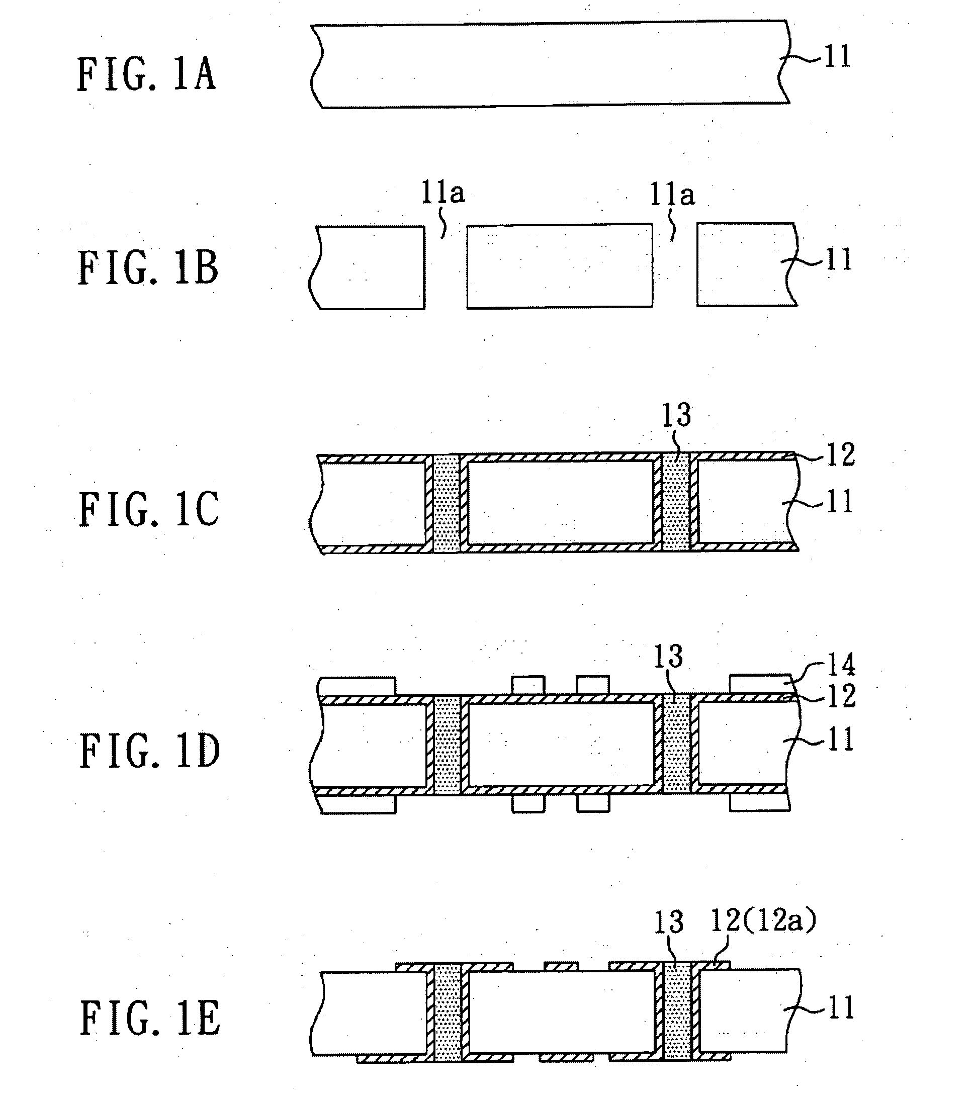
[0056]In FIG. 2A, an aluminum oxide board 21 is provided first as a core board of a flip-chip substrate. Then, a resist layer 22 is formed on the top surface 21a and the bottom surface 21b of the aluminum oxide board 21, as shown in FIG. 2B. The resist layer 22 used in this embodiment is a dry film. Subsequently, a plurality of openings 22a in the resist layer 22 is formed by photolithography, as shown in FIG. 2C.

[0057]After completing the above steps, part of the aluminum oxide board 21 not covered by the resist layer 22 is dissolved by electrolysis to form a plurality of through holes 21c, which penetrate the cross-section of the aluminum oxide board 21, as shown in FIG. 2D. Then, with reference to FIG. 2E, the resist layer 22 is removed so that the aluminum oxide board 21 having a plurality of through holes 21 is obtaine...

embodiment 2

[0065]In this embodiment, an aluminum oxide board is obtained by oxidizing an aluminum board for reduce the producing cost, because the aluminum board, which has low price and good processing property, is suitable for mass-producing and can be transformed into an aluminum oxide board by a simple method, such as oxidizing.

[0066]As shown in FIG. 3A, an aluminum board is provided first. Then, with reference to FIG. 3B, the aluminum board 51 is oxidized to be a non-conductive aluminum oxide board 21 by backing in the air. Further, the procedure illustrated in FIGS. 2B to 2N of embodiment 1 is proceeded to obtain a flip-chip substrate. Therefore, detailed steps of the procedure illustrated in FIGS. 2B to 2N are not described herein.

embodiment 3

[0067]As in embodiment 2, the method for manufacturing a flip-chip substrate of this embodiment is started by providing an aluminum board 51 first, as shown in FIG. 4A.

[0068]Then, with regard to FIG. 4B, a resist layer 52 is formed on the top surface 51a and bottom surface 51b of the aluminum board 51. The resist layer 52 used in this embodiment is a dry film. Subsequently, as shown in FIG. 4C, a plurality of openings 52a is formed in the resist layer 52 by development.

[0069]After the above steps, referring to FIG. 4D, the aluminum board 51 is electrolyzed to solve part of the aluminum board 51 not covered by the resist layer 52 so as to form a plurality of through holes 51c penetrating the cross-section of the aluminum board 51. Further, as shown in FIG. 4E, the resist layer 52 is removed so that a plurality of through holes 51c is obtained. In this embodiment, the through holes 51c are located corresponding to each of the openings 52a and formed by electrolysis. Therefore, the dia...


PUM


Abstract

A flip-chip substrate is disclosed, which comprises a core substrate including an aluminum oxide substrate and a first circuit layer, wherein the aluminum oxide substrate has a top surface, a bottom surface, and a plurality of conductive through holes, the conductive through holes connect the top surface and the bottom surface the first circuit layer disposed on the top surface and the bottom surface and electrically connects to the conductive through holes; and a built-up structure disposed on the top surface and the bottom surface and electrically connecting to the first circuit layer. Moreover, the conductive through holes are formed by forming plural through holes through electrolyzing, and then forming a first seed layer and a first metal layer inside the through holes. Therefore, the problem of substrate warpage can be prevented, and the wiring density of the flip-chip substrate can be improved.

Description

BACKGROUND OF THE INVENTION[0001]1. Field of the Invention[0002]The present invention relates to a flip-chip substrate, and, more particularly, to a flip-chip substrate capable of avoiding substrate warpage.[0003]2. Description of Related Art[0004]As the electronic industry develops rapidly, research moves towards electronic devices with multifunctions and high efficiency. Hence, circuit boards with many active and passive components and circuit connections thereon have been transformed from double-layered boards to multiple-layered boards so that the requirements such as integration and miniaturization in semiconductor packaging substrate can be met. Furthermore, interlayer connection technique is also applied in this field to expand circuit layout space in a limited circuit board and to meet the demand of the application of high-density integrated circuits.[0005]For manufacturing conventional semiconductor packaging structures, a chip is mounted on the top surface of a substrate f...

Claims


Application Information

Patent Timeline
IPC IPC(8): H05K1/09
CPCH01L21/486H01L23/15H01L23/49827H05K1/0306H05K3/108H05K3/423H05K3/4605H01L2924/0002H05K2201/09536H05K2201/09563H05K2201/096H01L2924/00
Inventor SHIH, CHAO-WEN
Owner PHOENIX PRECISION TECH CORP
Why Eureka
Try Eureka