Light emitting device

a technology of light-emitting devices and light-emitting elements, which is applied in the direction of basic electric elements, semiconductor devices, electrical equipment, etc., can solve the problems of significant emission efficiency impairment, difficult to achieve emission wavelengths of 500 nm or longer, and known vulnerability of active layers to heat damage, etc., to suppress or prevent disturbance of polarization, small unevenness

Inactive Publication Date: 2008-09-25
ROHM CO LTD
View PDF1 Cites 59 Cited by
  • Summary
  • Abstract
  • Description
  • Claims
  • Application Information

AI Technical Summary

Benefits of technology

[0022]The light emitting element may be configured such that the light may be extracted from a side of the group III nitride semiconductor substrate. According to this configuration, the light generated from the substrate can be extracted efficiently.
[0023]It is preferable that the light extract surface of the light emitting element is a mirror surface. The mirror surface is a surface having a small unevenness in comparison w

Problems solved by technology

When an active layer having an emission wavelength in a long wavelength band of 500 nm or longer is formed in a group III nitride semiconductor, such an active layer is known for vulnerability to heat damage.
The active layer undergoes heat damage in this instance, and emission efficiency is impaired significantly.
It is the

Method used


Image

  • Light emitting device
  • Light emitting device
  • Light emitting device

Examples


Embodiment Construction

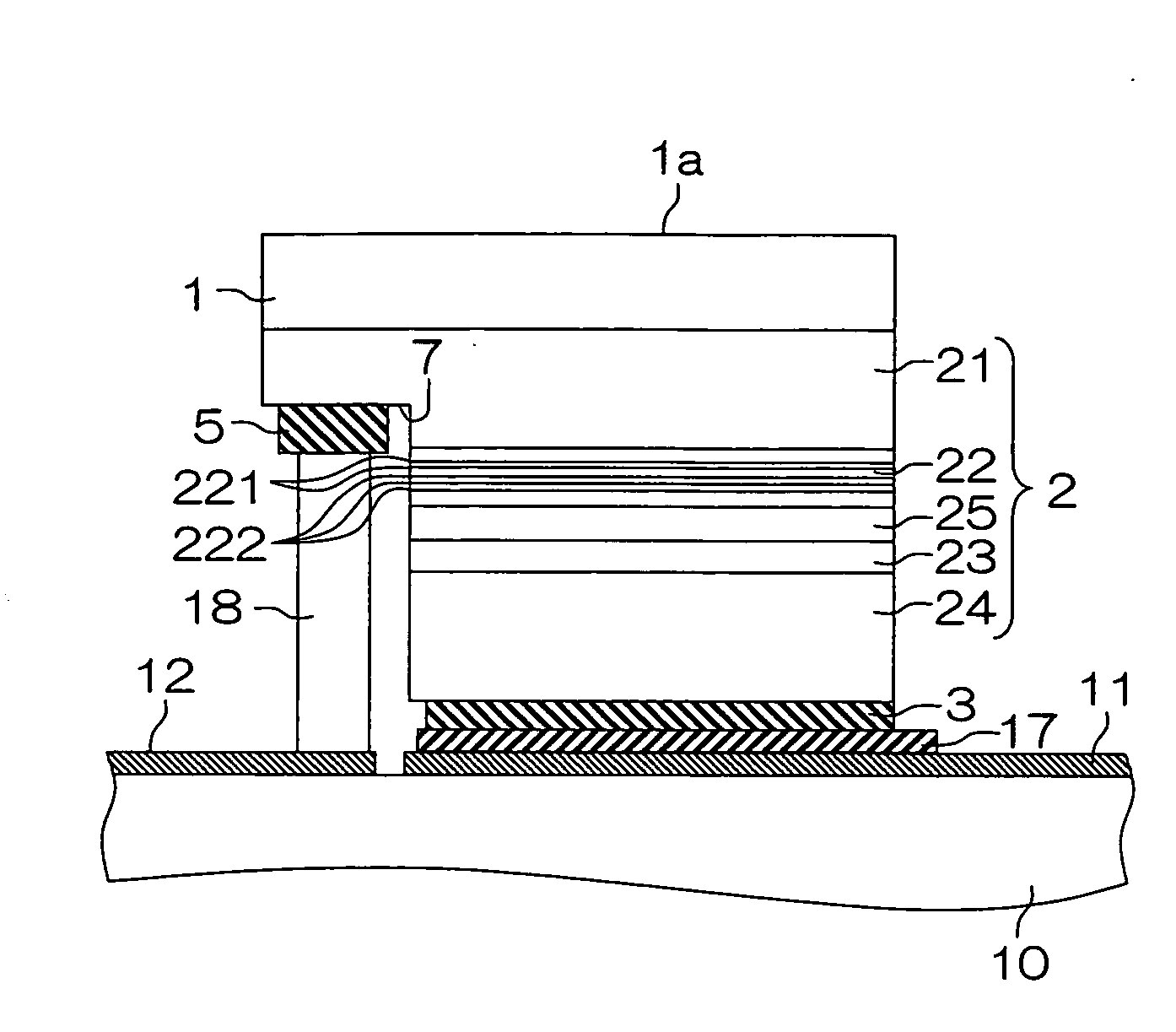
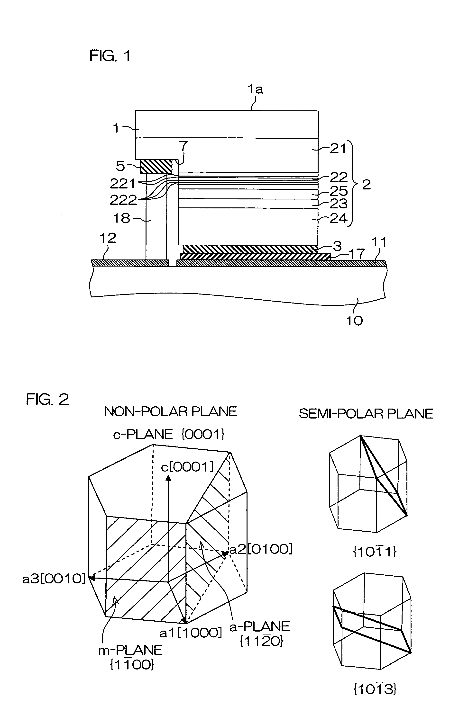
[0029]FIG. 1 is a schematic cross section describing the structure of a nitride semiconductor light emitting element according to one embodiment of the invention. The nitride semiconductor light emitting element is formed by growing a group III nitride semiconductor layer 2 as a group III nitride semiconductor laminating structure forming a light emitting diode structure on one principal plane (the bottom surface in FIG. 1) of a GaN (gallium nitride) substrate 1 as an example of a group III nitride semiconductor substrate.

[0030]The group III nitride semiconductor layer 2 has a laminating structure formed by sequentially laminating, from the GaN substrate 1 side, an n-type contact layer 21, a multiple-quantum well (MQW) layer 22 as an active layer (emission layer), a GaN final barrier layer 25, a p-type electron block layer 23, and a p-type contact layer 24. An anode electrode (p-type electrode) 3 is formed on the surface of the p-type contact layer 24. Further, a cathode electrode (...


PUM


Abstract

A light emitting element includes a group III nitride semiconductor substrate that emits a light by absorbing a UV ray and a light emitting diode structure. The light emitting diode structure is formed of a group III nitride semiconductor grown on the group III nitride semiconductor substrate, and has a p-type layer, an active layer that emits a light having a wavelength in the UV region, and an n-type layer. It is preferable that the group III nitride semiconductor substrate has a principal plane of a non-polar plane or a semi-polar plane and the group III nitride semiconductor having a same plane orientation as that of the principal plane is grown on the principal plane.

Description

BACKGROUND OF THE INVENTION[0001]1. Field of the Invention[0002]The present invention relates to a light emitting element having a light emitting diode structure using a nitride semiconductor.[0003]2. Description of Related Art[0004]Of the group III-V semiconductors, semiconductors using nitrogen as group V elements are referred to as group III nitride semiconductors. Representative examples are aluminum nitride (AlN), gallium nitride (GaN), and indium nitride (InN). Generally, they are expressed as AlxInyGa1-x-yN, where 0≦x≦1, 0≦y≦1, and 0≦x+y≦1.[0005]A manufacturing method of a nitride semiconductor has been known to grow group III nitride semiconductor on a gallium nitride (GaN) substrate having the principal plane in c-plane by metal organic chemical vapor deposition (MOCVD). By adopting this method, it is possible to form a GaN semiconductor laminating structure having an n-type layer and a p-type layer to fabricate a light emitting device using this laminating structure. Such ...

Claims


Application Information

Patent Timeline
IPC IPC(8): H01L33/00H01L29/06H01L33/06H01L33/16H01L33/32
CPCH01L33/02H01L33/502H01L33/16H01L33/08H01L2224/14H01L2224/16225
Inventor OKAMOTO, KUNIYOSHIOHTA, HIROAKI
Owner ROHM CO LTD
Why Eureka
Try Eureka