Pn Junction Type Group III Nitride Semiconductor Light-Emitting Device

Active Publication Date: 2008-09-25
TOYODA GOSEI CO LTD
View PDF47 Cites 22 Cited by
  • Summary
  • Abstract
  • Description
  • Claims
  • Application Information

AI Technical Summary

Benefits of technology

[0017]Further, a well layer which is not intentionally doped with impurities is joined to the oth

Problems solved by technology

However, in the above conventional techniques, the one end and the other end of the light-emitting layer are not limited to the barrier layers, and when one of the ends is a well layer, a carrier (electron) is prone to be dispersed toward the clad layer through the well layer, and there is a problem that the light emitting output is reduced by the same amount.
Ev

Method used


Image

  • Pn Junction Type Group III Nitride Semiconductor Light-Emitting Device
  • Pn Junction Type Group III Nitride Semiconductor Light-Emitting Device
  • Pn Junction Type Group III Nitride Semiconductor Light-Emitting Device

Examples


example 1

[0053]The present invention will be described concretely based on a case in which a Group III nitride semiconductor light emitting diode is produced using a light-emitting layer of multiple quantum well structure of the present invention formed on a sapphire substrate.

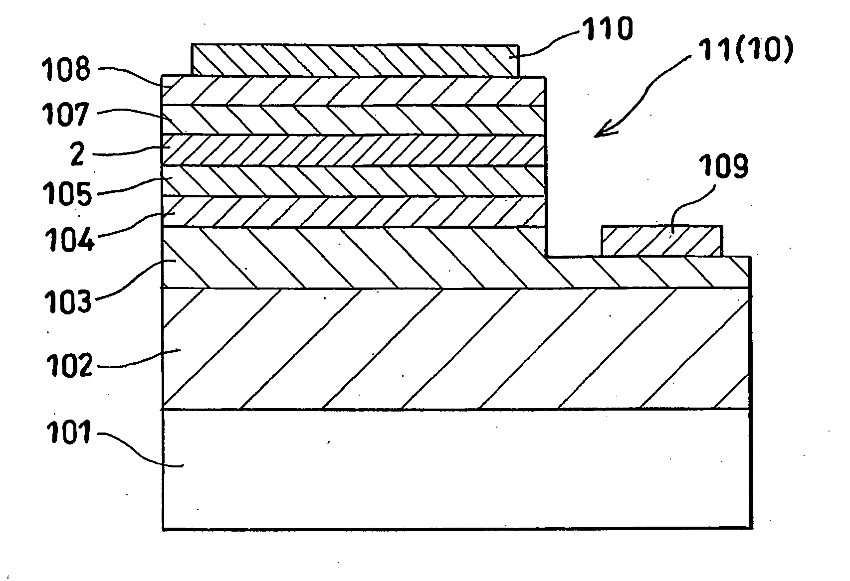
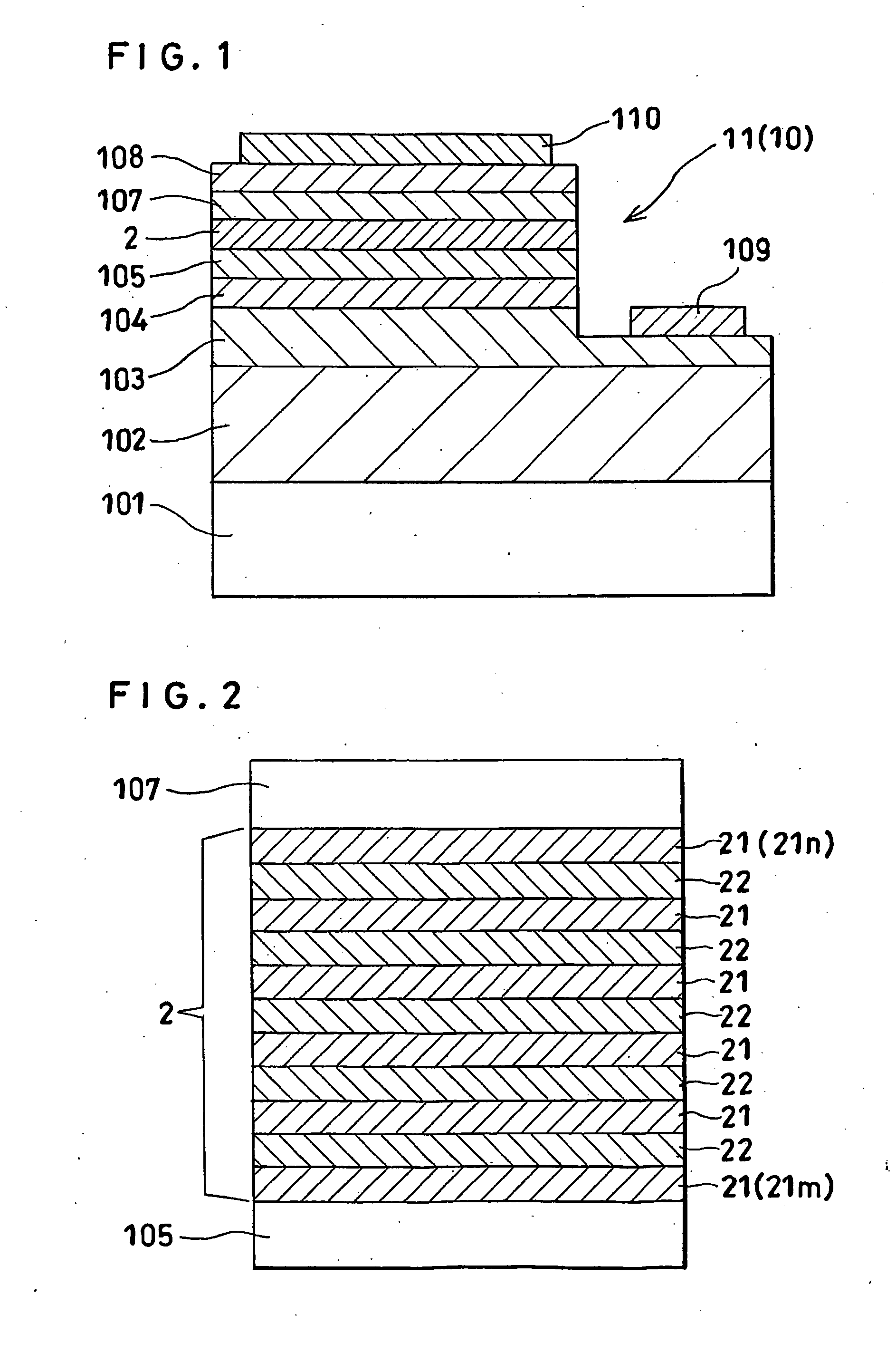
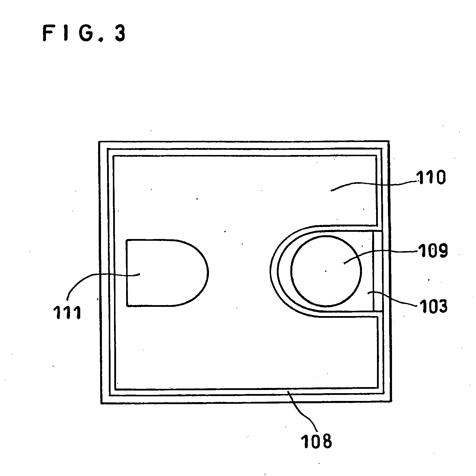
[0054]FIG. 1 is a schematic sectional view of a stacked structure used for producing the LED of Example 1. FIG. 2 is a schematic diagram showing a structure of the light-emitting layer of the stacked structure shown in FIG. 1. FIG. 3 is a schematic plan view of the LED produced from the stacked structure shown in FIG. 1.

[0055]To form a stacked structure 11 for producing an LED 10, a sapphire substrate 101 was placed in a quartz MOCVD reaction furnace around which an induction heating radio frequency (RF) coil was disposed. Nitrogen gas was allowed to flow therein for 10 minutes to purge the inside of the reaction furnace and then, the temperature of the substrate 101 was increased from the room temperature to 1150° C. ...

example 2

[0073]In Example 2, the contents of the present invention will be explained concretely based on a case in which a Group III nitride LED is formed using the light-emitting layer of multiple quantum well structure having barrier layers. The thicknesses of the barrier layers are different from one another.

[0074]In Example 2, in forming the multiple quantum well structure constituting the light-emitting layer described in Example 1, the thickness of the barrier layer of the one end layer (21m in FIG. 2) was set to 15 nm, that of the second barrier layer was set to 16 nm, that of the third barrier layer was set to 17 nm, thickness of the fourth barrier layer was set to 18 nm, and that of the fifth barrier layer was set to 19 nm.

[0075]That is, the multiple quantum well structure was formed, with the thicknesses of the Si dope GaN barrier layers reduced from the n-type clad layer (105 in FIGS. 1 and 2) toward the p-type clad layer (107 in FIGS. 1 and 2). The thickness of the Si dope GaN ba...

example 3

[0077]The present invention will be described concretely based on a case in which a Group III nitride semiconductor layer is formed using a light-emitting layer of multiple quantum well structure utilizing as the other end layer a barrier layer in which impurities were distributed.

[0078]In Example 3, the other end layer 21n forming the multiple quantum well structure described in Example 1 was made of an Si-doped GaN layer in which the concentration of Si impurities was set to be low on the side of the junction region with respect to the well layer, was higher at the central portion of the layer, and was gradually reduced from the central portion in the thickness-increasing direction (toward the p-type clad layer 107).

[0079]In the other end layer, the concentration of Si impurities from the junction region with respect to the well layer to an internal region of 5 nm in the thickness-increasing direction was set to 3×1017 cm−3. The concentration of Si impurities in a central region o...


PUM


Abstract

A pn junction type Group III nitride semiconductor light-emitting device 10 (11) of the present invention has a light-emitting layer 2 of multiple quantum well structure in which well layers 22 and barrier layers 21 including Group III nitride semiconductors are alternately stacked periodically between an n-type clad layer 105 and a p-type clad layer 107 which are formed on a crystal substrate and which include Group III nitride semiconductors, in which one end layer 21m of the light-emitting layer 2 is closest to and opposed to the n-type clad layer, and the other end layer 21n of the light-emitting layer 2 is closest to and opposed to the p-type clad layer, both the one and the other end layers are barrier layers, and the other end layer 21n is thicker than the barrier layer of the one end layer.

Description

CROSS REFERENCE TO RELATED APPLICATIONS [0001]This application is an application filed under 35 U.S.C. §111(a) claiming the benefit pursuant to 35 U.S.C. §119(e) (1) of the filing date of Provisional Application No. 60 / 553,533 filed Mar. 17, 2004 pursuant to 35 U.S.C §111(b).TECHNICAL FIELD [0002]The present invention relates to a pn junction type Group III nitride semiconductor light-emitting device having a light-emitting layer of multiple quantum well structure in which well layers and barrier layers including Group III nitride semiconductors are alternately stacked periodically between an n-type clad layer and a p-type clad layer which are formed on a crystal substrate and which include Group III nitride semiconductors.BACKGROUND ART [0003]Conventionally, the Group III nitride semiconductor is utilized as function material for constituting a Group III nitride semiconductor light-emitting device of pn hetero junction structure, such as a light-emitting diode (LED), which radiates...

Claims


Application Information

Patent Timeline
IPC IPC(8): H01L33/00H01L33/06H01L33/32H01S5/20H01S5/323H01S5/343
CPCB82Y20/00H01L33/06H01S5/34333H01S5/2009H01S5/309H01L33/32
Inventor YASUDA, TAKAKITOMOZAWA, HIDEKI
Owner TOYODA GOSEI CO LTD
Why Eureka
Try Eureka