
Molybdenum barrier metal for SiC Schottky diode and process of manufacture

a technology of molybdenum barrier and sic, which is applied in the direction of basic electric elements, electrical apparatus, and devices with poor comparison performance, can solve the problems of performance degradation defects in the sic epilayer of high-voltage versions, currently available sic-sbds that do not fully realize the high performance potential of sic, and achieve better forward conduction performance, reduce the height barrier value, and limit the effect of electric field strength

Active Publication Date: 2008-10-02
VISHAY SILICONIX LLC
View PDF94 Cites 30 Cited by
  • Summary
  • Abstract
  • Description
  • Claims
  • Application Information

AI Technical Summary

Benefits of technology

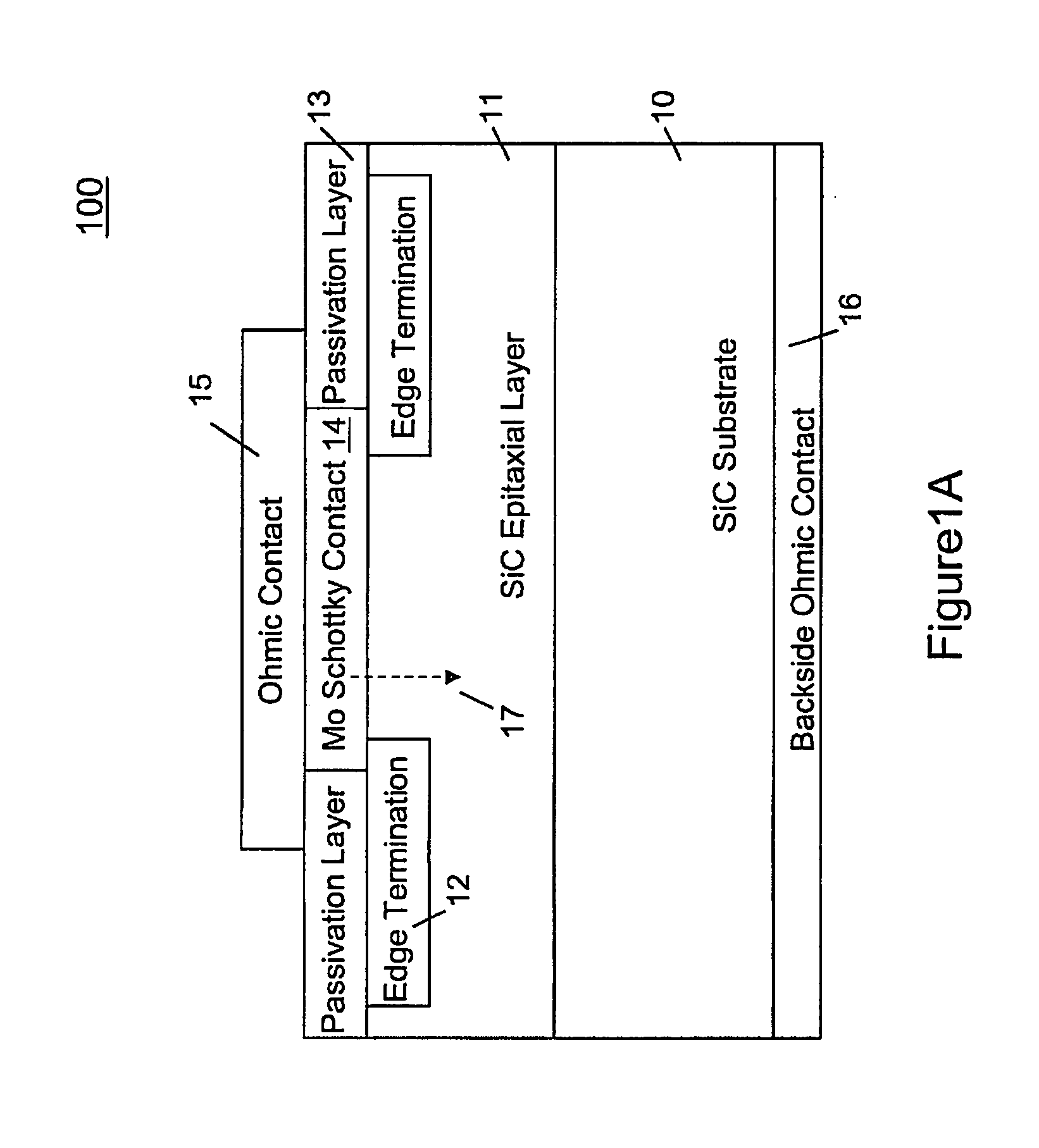
[0008]A molybdenum Schottky contact is disclosed that provides an improvement, as compared to titanium and other potential Schottky contact materials, in forward current conduction and reverse voltage blocking performance. Additionally, the molybdenum Schottky contact provides greater device operating stability at high temperatures and allows a higher annealing temperature than does SiC Schottky diodes that use titanium (Ti) or nickel (Ni) Schottky contacts.
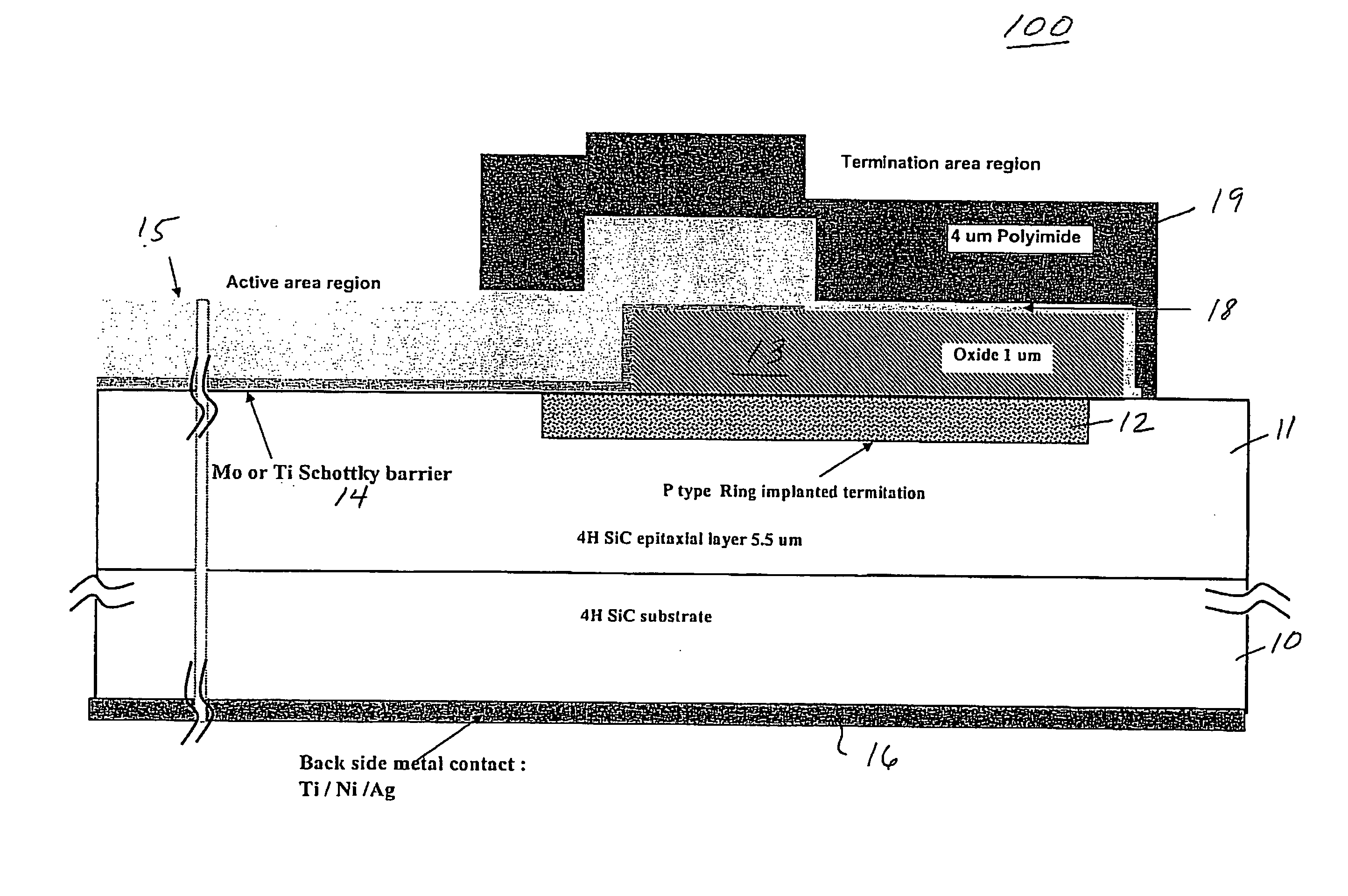
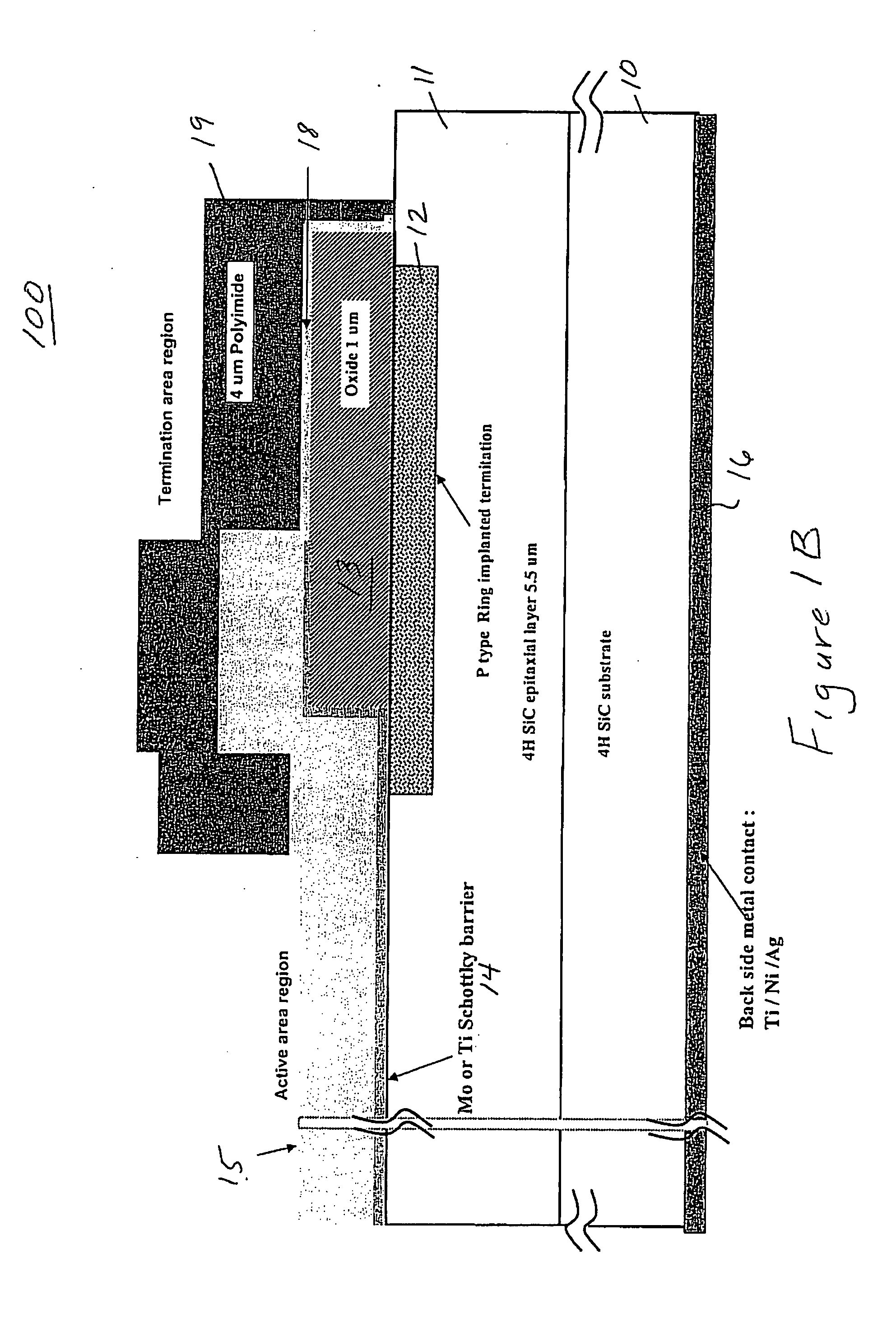
[0015]In one embodiment, Schottky barrier diodes with Mo as the Schottky barrier exhibit a blocking voltage similar to that obtained by standard Ti metallization but with a lower height barrier value. A consequence of the lower barrier value is a better performance in forward conduction as is shown in FIG. 2A as well as in reverse or blocking voltage as shown in FIG. 2B. Moreover, junction barrier Schottky diodes limit the electric field strength on the Schottky barrier and thus limit Schottky barrier lowering and reverse current flow.

Problems solved by technology

Challenges to the successful manufacture of such devices include intrinsic properties of the materials used to fabricate the devices and physical defects that may be present in those materials.
However, these devices demonstrate poor performance in comparison with the ideal performance potential of SiC.
More specifically, currently available SiC-SBDs do not fully realize the high performance (high-voltage, high current capacity, and low-loss) potential of SiC.
In addition, currently available SiC-SBDs exhibit performance degrading defects in the SiC epilayer of high-voltage versions.

Method used


Image

  • Molybdenum barrier metal for SiC Schottky diode and process of manufacture
  • Molybdenum barrier metal for SiC Schottky diode and process of manufacture
  • Molybdenum barrier metal for SiC Schottky diode and process of manufacture

Examples


Embodiment Construction

[0024]The present invention will now be described in detail with reference to a various embodiments thereof as illustrated in the accompanying drawings. In the following description, specific details are set forth in order to provide a thorough understanding of the present invention. It will be apparent, however, to one skilled in the art, that the present invention may be practiced without using some of the implementation details set forth herein. It should also be understood that well known operations have not been described in detail in order to not unnecessarily obscure the present invention.

Molybdenum Barrier Metal for SiC Schottky Diode and Process of Manufacture According to One Embodiment of the Present Invention

[0025]FIG. 1A shows a cross-section of a silicon carbide (SiC) Schottky barrier diode (SBD) 100 fabricated according to one embodiment of the invention. In one embodiment, a molybdenum (Mo) Schottky contact is used that provides an improvement, as compared to tita...


PUM


Abstract

A method for fabricating a diode is disclosed. In one embodiment, the method includes forming a Schottky contact on an epitaxial layer of silicon carbide (SiC) and annealing the Schottky contact at a temperature in the range of 300° C. to 700° C. The Schottky contact is formed of a layer of molybdenum.

Description

RELATED U.S. APPLICATIONS[0001]This application claims priority to co-pending provisional application Ser. No. 60 / 820,807 filed on Jul. 31, 2006, which is hereby incorporated by reference to this specification.FIELD OF THE INVENTION[0002]This invention relates to a silicon carbide (SiC) Schottky diode with a molybdenum Schottky barrier contact.BACKGROUND[0003]A diode is an electronic component that restricts the direction of flow of electric current. More specifically, it allows electric current to flow in one direction, but blocks electric current flow in the opposite direction. Accordingly, a diode can be thought of as an electronic version of a mechanical check valve. Circuits that require current flow in only one direction typically include one or more diodes.[0004]Schottky diodes are diodes that are formed from the contact between a metal and a semiconductor rather than from a p-n junction. They have a lower forward voltage drop than a standard p-n junction diode. Schottky diod...

Claims


Application Information

Patent Timeline
IPC IPC(8): H01L29/24H01L21/04
CPCH01L29/47H01L29/0619H01L29/6606H01L29/872H01L29/1608
Inventor RICHIERI, GIOVANNI
Owner VISHAY SILICONIX LLC
Learn More