

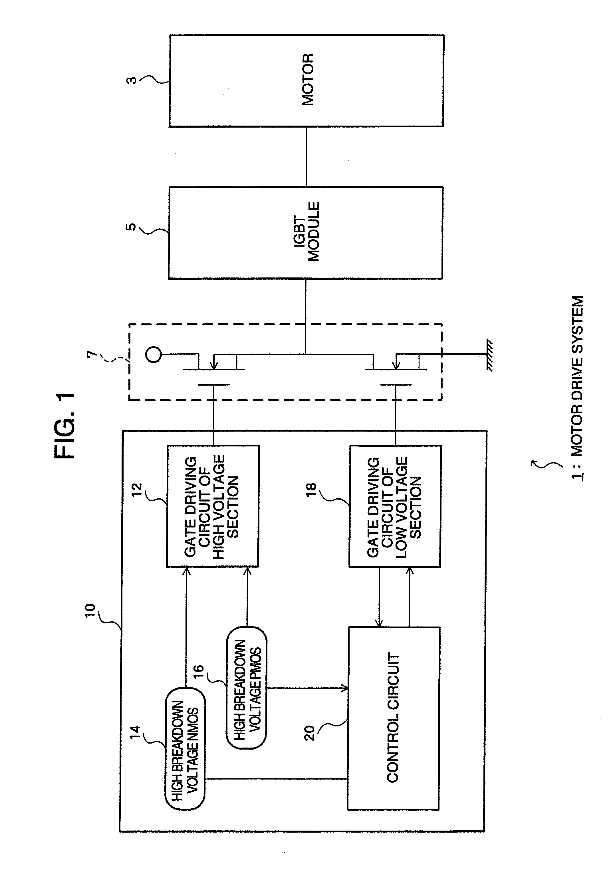
High breakdown voltage semiconductor circuit device and method of manufacturing the same
a semiconductor circuit and high breakdown voltage technology, applied in the field of semiconductor circuit devices, can solve the problem of inability to shorten the gate electrode, and achieve the effect of high integration and high breakdown voltage and high breakdown voltag
- Summary
- Abstract
- Description
- Claims
- Application Information
AI Technical Summary
Benefits of technology
Problems solved by technology
Method used
Image

Examples
embodiment 1
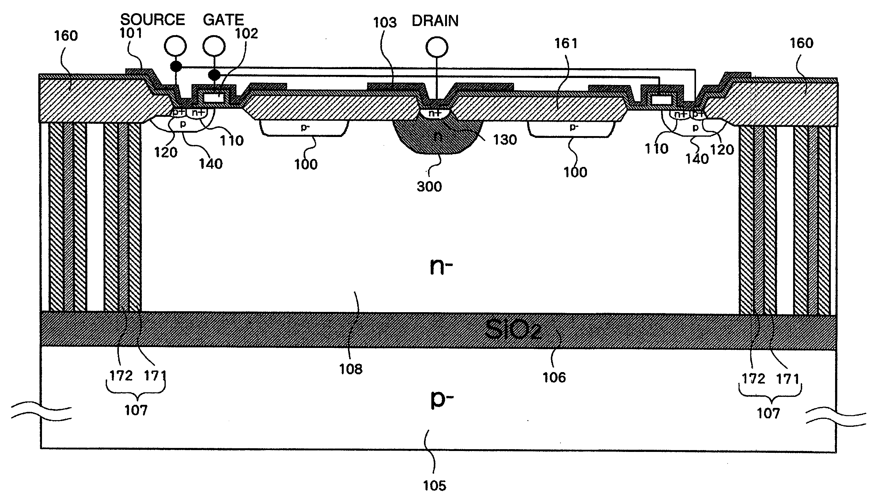
[0048]First, the details of the dielectric isolation semiconductor device 10 in accordance with a first embodiment of the present invention will be described referring to FIGS. 2 and 3.
[0049]FIG. 2 is a cross-sectional view showing the dielectric isolation semiconductor device 10 in accordance with the first embodiment. In the first embodiment, the present invention is applied to a dielectric isolation semiconductor device including a high breakdown voltage n-MOS transistor provided with an n-type channel. In FIG. 2, elements other than the n-MOS transistor are omitted for brevity. Incidentally, while a p-type semiconductor is employed for a semiconductor substrate, especially the silicon support substrate 105, in this embodiment, it is also possible to employ an n-type semiconductor for the semiconductor substrate.
[0050]The so-called “SOI substrate” is formed by stacking a high-resistance (i.e. low impurity concentration) n-type silicon active layer 108 on the silicon support subst...
embodiment 2
[0073]First, a dielectric isolation semiconductor device in accordance with a second embodiment of the present invention will be described below.
[0074]FIG. 7 is a cross-sectional view showing the principal part of the dielectric isolation semiconductor device in accordance with the second embodiment. In the dielectric isolation semiconductor device of the second embodiment, a p-type impurity diffusion region 200 is formed on the inner side face of the dielectric isolation region 107.
[0075]The p-type impurity diffusion region 200 makes contact with the p-type channel region 140 in the vicinity of the silicon surface. In this embodiment, when reverse voltage is applied between the source and the drain, the spread of the depletion layer from the source side starts from the p-type channel region 140 and the p-type impurity diffusion region 200, thereby the spread of the depletion layer in the horizontal direction is facilitated in comparison with the structure in the first embodiment. T...
embodiment 3
[0076]Next, a dielectric isolation semiconductor device in accordance with a third embodiment of the present invention will be described below.
[0077]FIG. 8 is a cross-sectional view showing the dielectric isolation semiconductor device in accordance with the third embodiment. The dielectric isolation semiconductor device of the third embodiment, employing the SOI substrate of the high breakdown voltage n-channel MOS (NMOS) transistor of the first embodiment, further includes a high breakdown voltage p-channel MOS (PMOS) transistor. While the NMOS transistor and the PMOS transistor are adjoining each other in FIG. 8, they may also be separated from each other as long as an NMOS transistor and a PMOS transistor are implemented on one SOI substrate. The PMOS transistor in this embodiment is configured in a region (area) surrounded by two dielectric isolation regions 270 which are formed simultaneously with, in the same structure as, and by the same process as the two dielectric isolati...
PUM
 Abstract
Description
Claims
Application Information