Semiconductor light-emitting device

a technology of semiconductors and light-emitting devices, which is applied in the direction of semiconductor devices, basic electric elements, electrical equipment, etc., can solve the problems of poor light reflectivity of materials commonly used for p-type semiconductor layers, and reducing the reflective effect of light, so as to achieve good ohmic contact, good ohmic contact, and high reflectivity

Inactive Publication Date: 2008-10-09
ADVANCED OPTOELECTRONICS TECH
View PDF1 Cites 94 Cited by
  • Summary
  • Abstract
  • Description
  • Claims
  • Application Information

AI Technical Summary

Benefits of technology

[0011]One aspect of the present invention is to provide a semiconductor light-emitting device with both high reflectivity and good ohmic contacts, and by disposing a material with good ohmic contact on the

Problems solved by technology

The materials commonly used for P-type semiconductor layer 14 with good ohmic contact, such as nickel/gold or gold, are often poor in light reflectivity, especially for light with shorter wavelengths such as blue light, violet light, and ultraviolet light.
If materials with better light reflectivity are used as the ohmic contact layer 15, for example, rhodium (Rh), palladium (Pd), and platinum (PT), although properties of good ohmic contact and fine reflectivity can both be achieved, they are mostly expensive and rare metals.
Furthermore, the deposition proces

Method used


Image

  • Semiconductor light-emitting device
  • Semiconductor light-emitting device
  • Semiconductor light-emitting device

Examples


Embodiment Construction

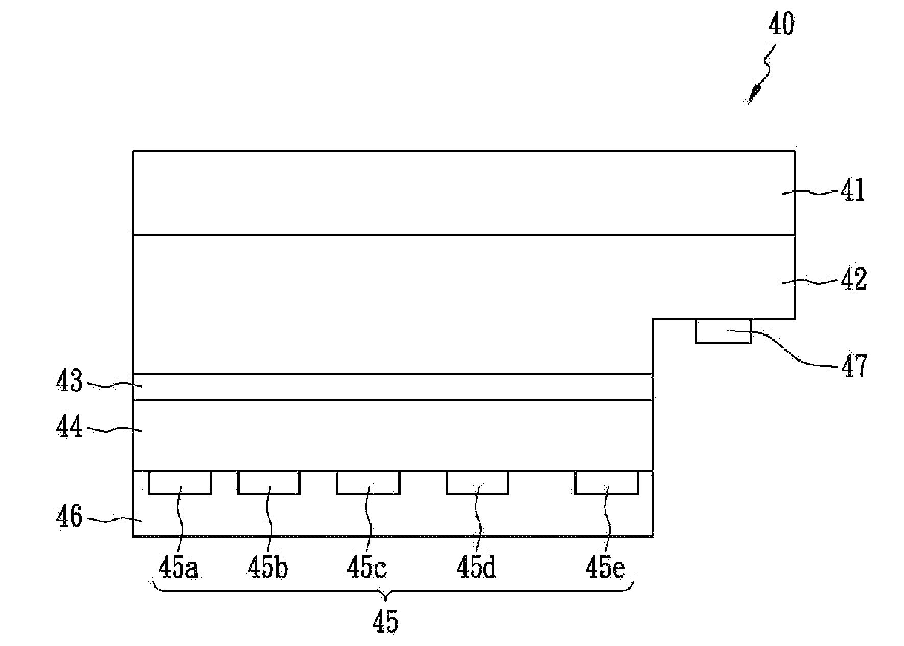
[0038]FIG. 4 is the cross-sectional diagram of the semiconductor light-emitting device of the present invention. An N-type semiconductor layer 42, an active layer 43, a P-type semiconductor layer 44, an ohmic contact layer 45, and a reflective layer 46 are sequentially formed on the sapphire substrate 41, and an N-type electrode 47 is formed on the exposed N-type semiconductor layer 42. The intervals between each ohmic contact block in blocks 45a to 45e on the ohmic contact layer 45 increase accordingly. By controlling the intervals between the ohmic contact blocks 45a to 45e and the distances of those blocks to the N-type electrode 47, one can compensate for the non-uniform potential distribution in the light-emitting structure caused by accumulated resistance in the N-type semiconductor layer 42, and subsequently create uniform current distribution in the light-emitting structure. The ohmic contact block 45 is formed through deposition of Ni / Au, Ni, Au, Rh, Pb, Pt, ITO, or IZO, an...


PUM


Abstract

A semiconductor light-emitting device comprises an N-type semiconductor layer, an active layer formed on the surface of the N-type semiconductor layer, a P-type semiconductor layer formed on the surface of the active layer, and a reflective layer formed on the surface of the P-type semiconductor layer. A plurality of ohmic contact blocks with electrical properties of ohmic contact are on the surface of the reflective layer adjacent to the P-type semiconductor layer, and the remaining part of the surface acts as the reflective regions with higher reflectivity, and the reflective regions can effectively reflect the light generated from the active layer.

Description

BACKGROUND OF THE INVENTION[0001](A) Field of the Invention[0002]The present invention relates to a semiconductor light-emitting device, and more particularly, to a photo-electronic semiconductor device comprising P-type ohmic contacts and reflective structures.[0003](B) Description of the Related Art[0004]Light-emitting diodes (LED) have been widely used in various products and have recently become an important research topic in photo-electronic semiconductor materials for producing blue light LED. Materials currently used for blue light LED include ZnSe, SiC, and InGaN etc., and those semiconductor materials exhibit band gap properties with the gap energy of approximately over 2.6 eV.[0005]As the GaN series of light-emitting materials exhibits direct gap properties, they are able to generate light with high luminance and have the advantage of longer lifetime compared to the other similar direct gap material, ZnSe. Furthermore, the range of the gap energy of the GaN series or other...

Claims


Application Information

Patent Timeline
IPC IPC(8): H01L33/00H01L33/38H01L33/40H01L33/46
CPCH01L33/387H01L33/405H01L33/46
Inventor HSU, CHIH PENGMA, CHIH PANGCHAN, SHIH HSIUNG
Owner ADVANCED OPTOELECTRONICS TECH
Why Eureka
Try Eureka