Semiconductor device including schottky barrier diode and method of manufacturing the same

a technology of schottky barrier and semiconductor device, which is applied in the direction of semiconductor devices, diodes, electrical apparatus, etc., can solve the problems of restricted concentration of electric fields, achieve high voltage resistance, reduce reverse current, and reduce current path between the first electrode and the second electrode

Inactive Publication Date: 2008-10-09
DENSO CORP
View PDF5 Cites 35 Cited by
  • Summary
  • Abstract
  • Description
  • Claims
  • Application Information

AI Technical Summary

Benefits of technology

[0017]In the semiconductor device manufactured by the above-described method, the plurality of first columns and the plurality of second columns configurate a super junction structure, and the first electrode and the plurality of first columns provide schottky barrier diodes in the super junction structure. Thus, a resistance of a current path between the first electrode and the second electrode is reduced. In addition, because the s

Problems solved by technology

In addition, because the semiconductor device has the super junct

Method used


Image

  • Semiconductor device including schottky barrier diode and method of manufacturing the same
  • Semiconductor device including schottky barrier diode and method of manufacturing the same
  • Semiconductor device including schottky barrier diode and method of manufacturing the same

Examples


first embodiment

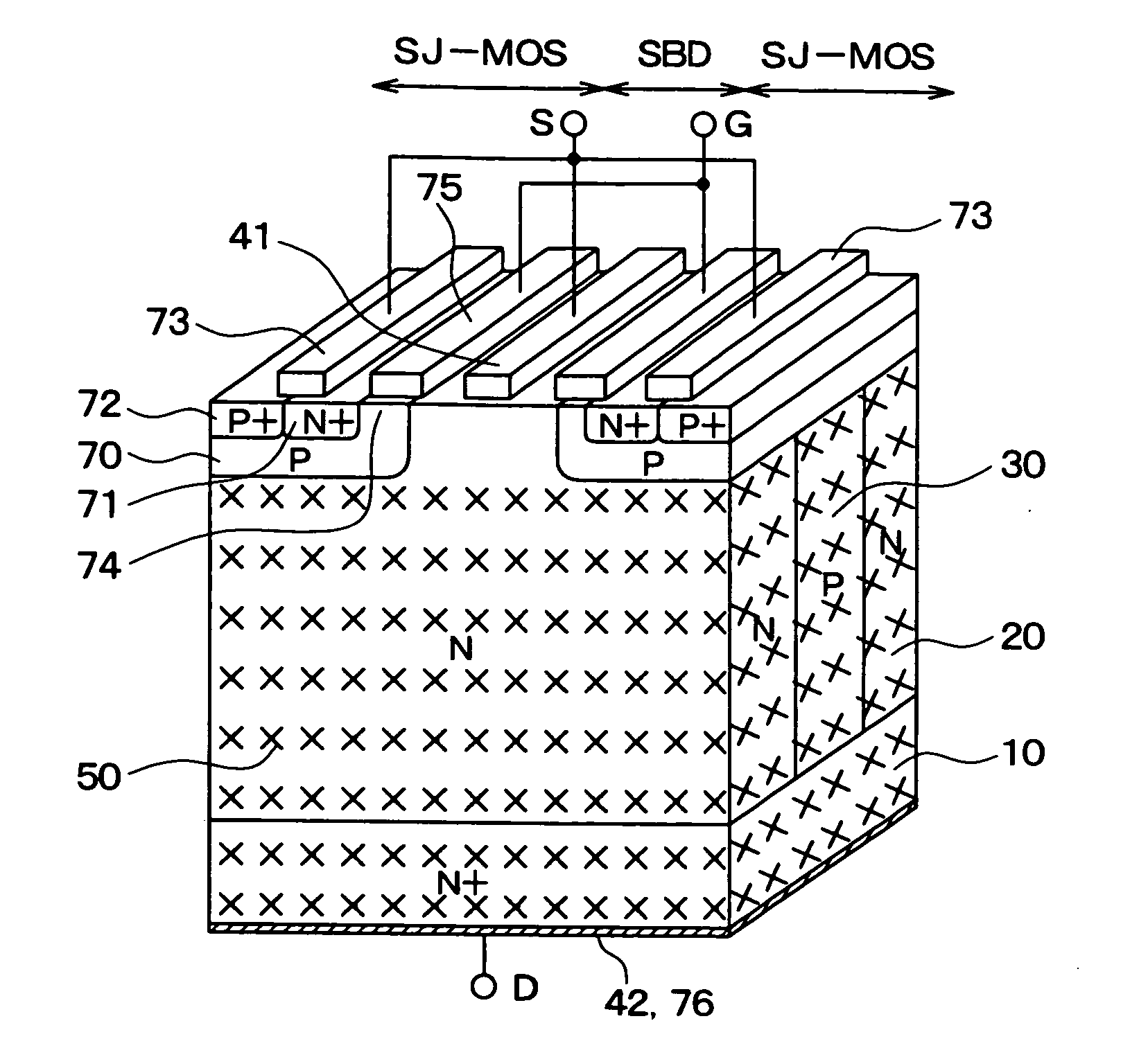
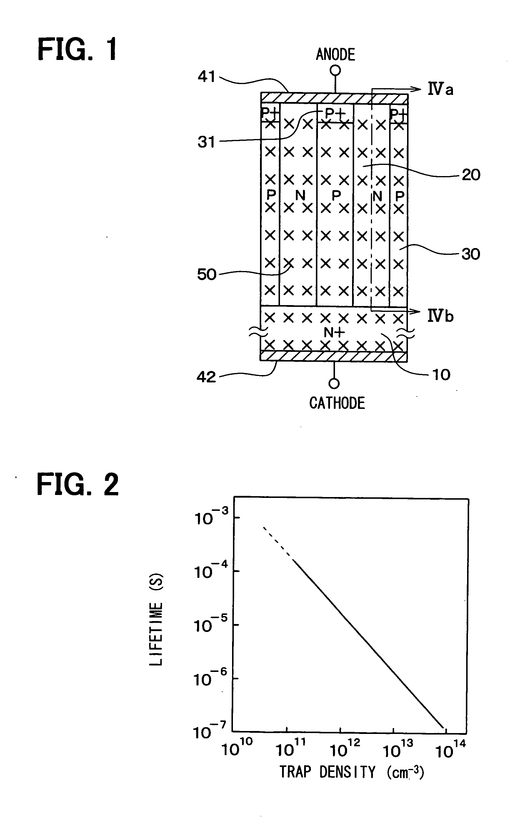
[0039]A semiconductor device according to a first embodiment of the invention will be described with reference to FIGS. 1-5.

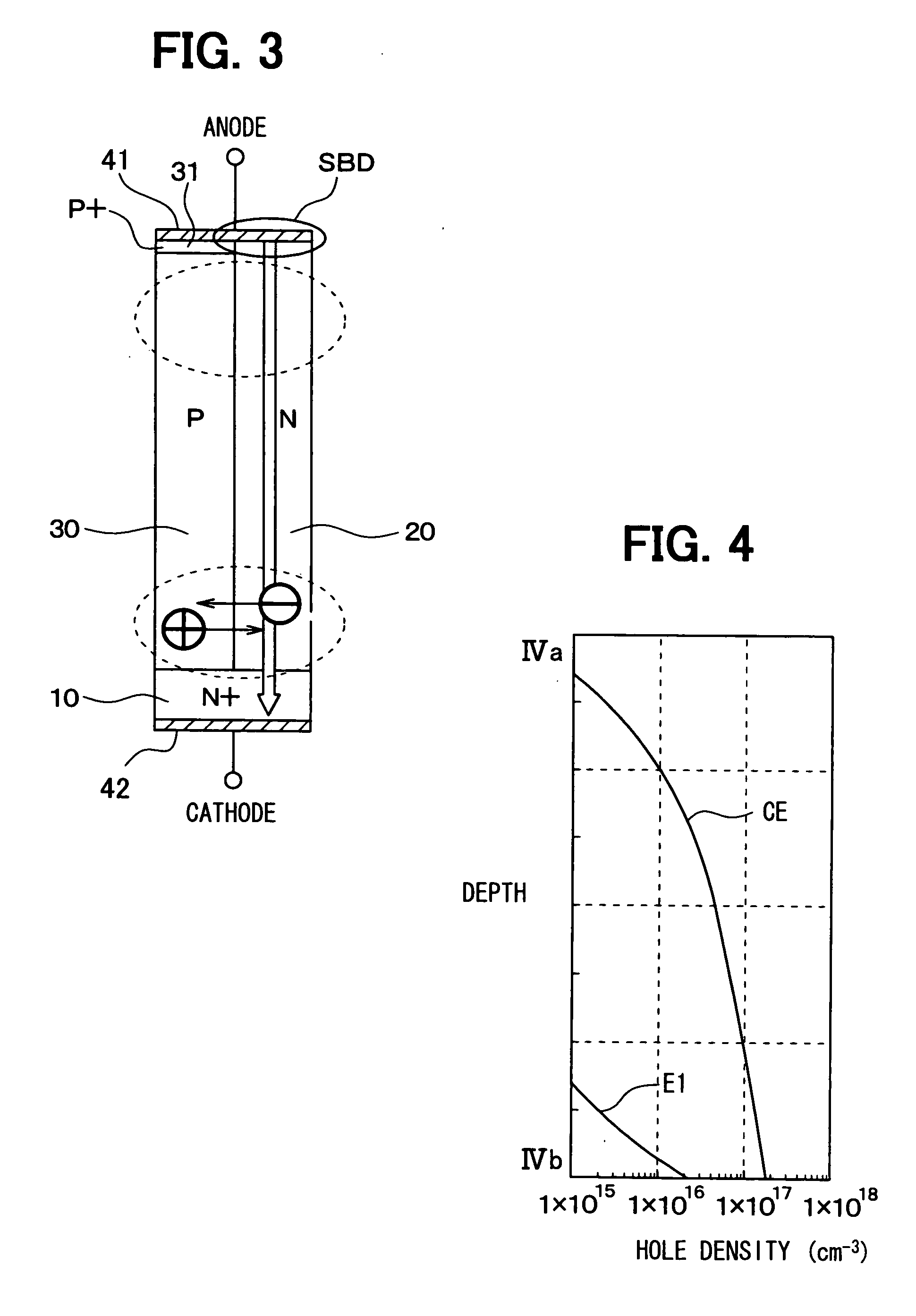
[0040]The semiconductor device has a super junction structure (SJ structure) including an N+ type substrate 10, N type regions (N column) 20 each having a column shape and P type regions (P column) 30 each having a column shape. On the N+ type substrate 10, the N columns 20 and the P columns 30 are alternately arranged in a plane direction of the N+ type substrate 10. That is, the semiconductor device shown in FIG. 1 has a repetition structure in which the N columns 20 and the P columns 30 are alternately arranged.

[0041]For example, the N+ type substrate 10 has an impurity concentration in a range from about 1×1018 cm−3 to about 1×1020 cm−3. Each of PN columns that includes the N column 20 and the P column 30 has an impurity concentration in a range from about 1×1015 cm−3 to about 1×1018 cm−3, a width in a range from about 0.1 μm to about 10 μm, a depth in a ra...

second embodiment

[0059]In the semiconductor device shown in FIG. 1, the whole SJ structure is formed as the lifetime control region 50. Alternatively, only the bottom portion of the SJ structure, at which the parasitic PN diode is provided, may be formed as the lifetime control region 50. Also in the present case, the reverse-recovering property can be improved.

[0060]In a semiconductor device according to a second embodiment of the invention, only a portion of the SJ structure on the side of the N+ type substrate 10, that is, only the bottom portion of the SJ structure is formed as the lifetime control region 50, as shown in FIG. 6. Other part of the semiconductor device shown in FIG. 6 is almost similar to the semiconductor device shown in FIG. 1.

[0061]In the present case, after forming the SJ structure on the N+ type substrate 10, for example, helium ion is irradiated from a side of the N+ type substrate 10 toward a side of the SJ structure, and thereby the lifetime control region 50 is provided a...

third embodiment

[0063]In a semiconductor device according to a third embodiment of the invention, each of the N columns 20 has an N− type region 21 at a surface portion thereof, as shown in FIG. 7. Each of the N− type regions 21 has a low impurity concentration compared with each of the N columns 20. For example, the N− type region 21 has an impurity concentration in a range from about 1×1014 cm−3 to about 1×1017 cm−3.

[0064]Other part of the semiconductor device shown in FIG. 7 is almost similar to the semiconductor device shown in FIG. 1. In the present case, the lifetime control region 50 is provided at the whole SJ structure. Thus, a low resistance, a high voltage resistance, and a high reverse-recovering property can be obtained.


PUM


Abstract

A semiconductor device includes a substrate, a plurality of first columns having a first conductivity type, a plurality of second columns having a second conductivity type, a first electrode, and a second electrode. The first columns and the second columns are alternately arranged on the substrate to provide a super junction structure. The first electrode is disposed on the super junction structure, forms schottky junctions with the first columns, and forms ohmic junctions with the second columns. The second electrode is disposed on the substrate on an opposite side of the super junction structure. At least a part of the substrate and the super junction structure has lattice defects to provide a lifetime control region at which a lifetime of a minority carrier is controlled to be short.

Description

CROSS REFERENCE TO RELATED APPLICATION[0001]This application is based on Japanese Patent Application No. 2007-97416 filed on Apr. 3, 2007, the contents of which are incorporated herein by reference in their entirety.BACKGROUND OF THE INVENTION[0002]1. Field of the Invention[0003]The present invention relates to a semiconductor device including a schottky barrier diode and a method of manufacturing the semiconductor device.[0004]2. Description of the Related Art[0005]Conventionally, an inverter circuit is used for driving an alternate current diode with a high efficiency, for example. An inverter circuit 80 according to an example of the related art includes switching elements 81 and freewheeling diodes 82, as shown in FIG. 19. The switching elements 81 and the freewheeling diodes 82 are coupled in parallel for driving a motor (not shown) at three phases including a U-phase, a V-phase, and a W-phase.[0006]For example, a low-loss insulated gate bipolar transistor (IGBT) may be used as...

Claims


Application Information

Patent Timeline
IPC IPC(8): H01L27/06H01L21/329H01L29/872
CPCH01L29/0634H01L29/0878H01L29/32H01L29/7806H01L29/861H01L29/872
Inventor SAKAKIBARA, JUNYAMAGUCHI, HITOSHI
Owner DENSO CORP
Why Eureka
Try Eureka