

Integrated passive device with a high resistivity substrate and method for forming the same
a technology of integrated passive devices and substrates, which is applied in the direction of basic electric elements, electrical apparatus, and semiconductor devices. it can solve the problems of increasing the difficulty of fitting all of the desired components into a single wireless device, low resistivity to be used, and materials considerably more expensive than silicon. achieve the effect of increasing the effective resistivity of silicon substrates and high resistivity
- Summary
- Abstract
- Description
- Claims
- Application Information
AI Technical Summary
Benefits of technology
Problems solved by technology
Method used
Image

Examples
Embodiment Construction
[0020]The following detailed description is merely exemplary in nature and is not intended to limit the invention or application and uses of the invention. Furthermore, there is no intention to be bound by any expressed or implied theory presented in the preceding technical field, background, brief summary, or the following detailed description. It should also be noted that FIGS. 1-15 are merely illustrative and may not be drawn to scale.
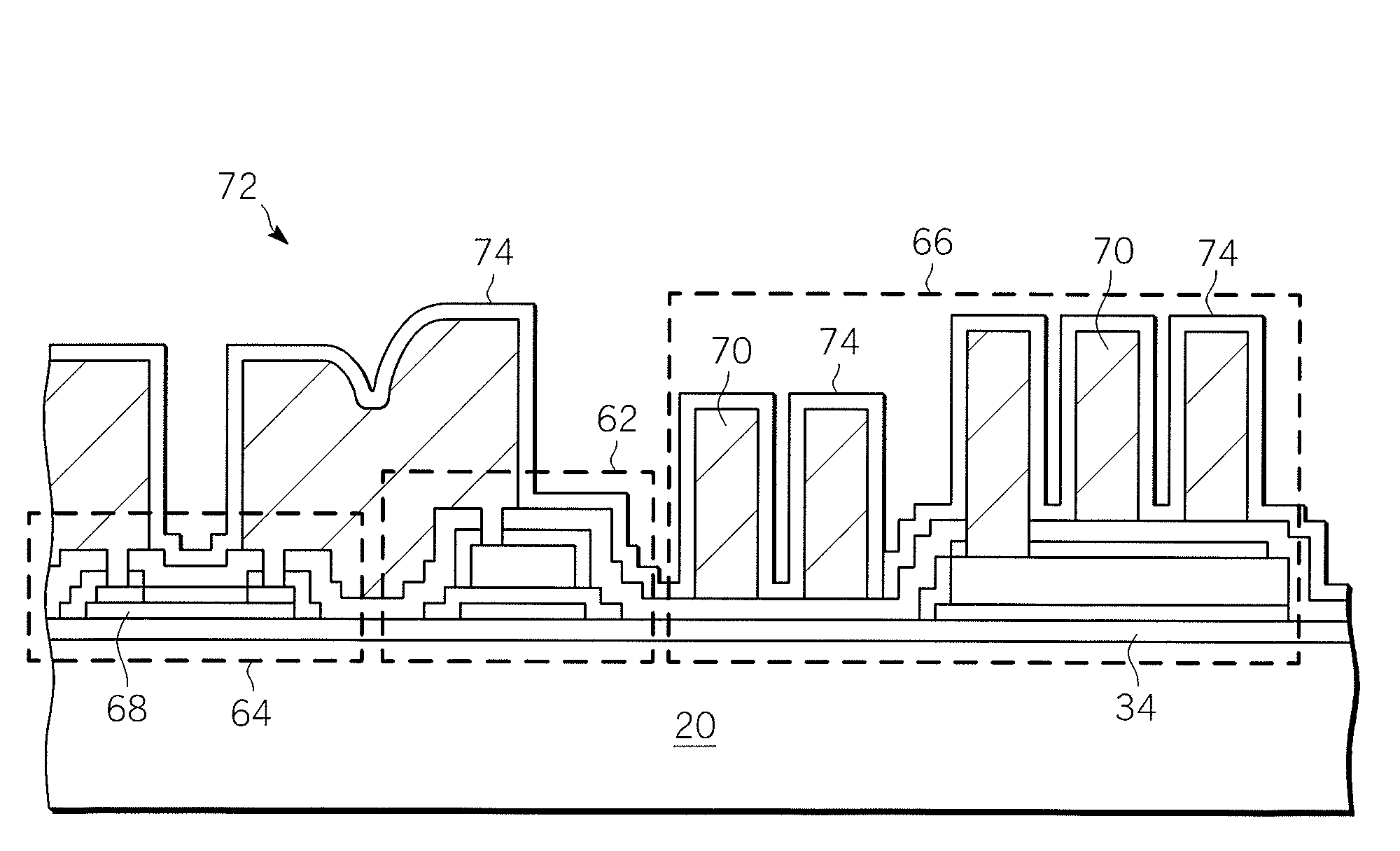
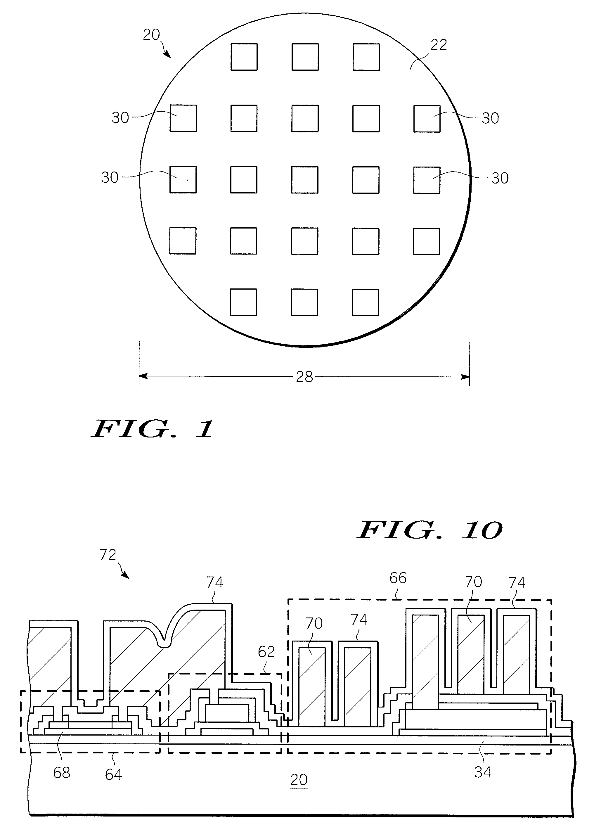
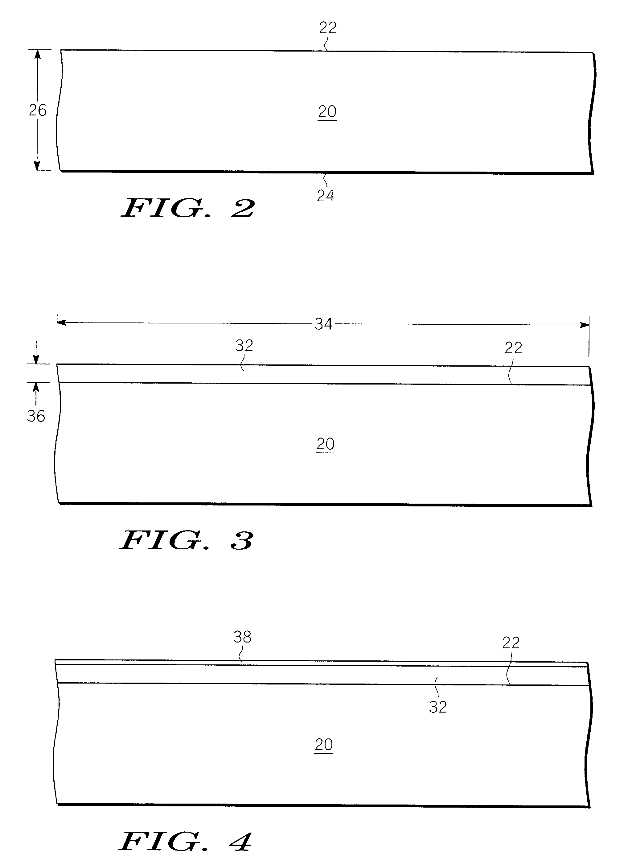
[0021]FIG. 1 to FIG. 11 illustrate a method for forming an integrated passive device (IPD). A relatively thick oxide layer is formed on a high resistivity silicon substrate, and at least one passive electronic component is formed over the oxide layer. The combination of the thickness (i.e., at least 4 micrometers (μm)) of the oxide layer, along with the resistivity of the oxide material, increases the effective resistivity of the silicon substrate so that the substrate is suitable for use in IPDs used in, for example, wireless communications devices...
PUM
 Abstract
Description
Claims
Application Information