Organic electroluminescent devices

Active Publication Date: 2008-10-09
TSINGHUA UNIV +2
View PDF5 Cites 11 Cited by
  • Summary
  • Abstract
  • Description
  • Claims
  • Application Information

AI Technical Summary

Benefits of technology

[0032]Without being limited with any theory, it can be believed that in some embodiments of the present invention, since the leads are transferred to the packaging sheet and bonded at the end of the packaging sheet, the area of luminescent region may not be influenced by the leads, so that the size of bonding frame can be reduced, the luminescent region is enlarged. In some embodiments, since electrode leads are sealed in the device, they are protected from effects of air, water and oxygen. As for some embodiments of the double-sided electroluminescent device, the packaging sheet as supporter not only provides a space for drying agent and heat dissipation, but also provides bonding regions for leads of luminescent components. In addition, some embodiments of the present invention can be implemented by a simple manufacture process, and since leads region and bonding region ar

Problems solved by technology

In a double-sided organic electroluminescent device module of the art, the bonding of leads is also performed on substrate, a packaging sheet is sandwiched between two light-emitting components for packaging, supporting drying and heat dispersion, so that such a device has a relatively large volume and a relatively broad frame after bonding, and is difficult in cutting procedure.
1) Uniformity of luminescence is poor: For example, as for points C and D in the luminescent region 32, since the point C is further from the lead bonding region 33 than the point D, the electric resistance from the bonding region 33 to the point C is greater than that to the point D, so that the electric current density at the point C is less than that at the point D during working, and the brightness at the point C is lower than that at the point D, i.e., the luminescence of the device is not uniform. In the meantime, the commonly used auxiliary electrodes are of metal Cr, while Cr layer has a relatively high surface resistance, so that it is difficult t

Method used


Image

  • Organic electroluminescent devices
  • Organic electroluminescent devices
  • Organic electroluminescent devices

Examples


example 1

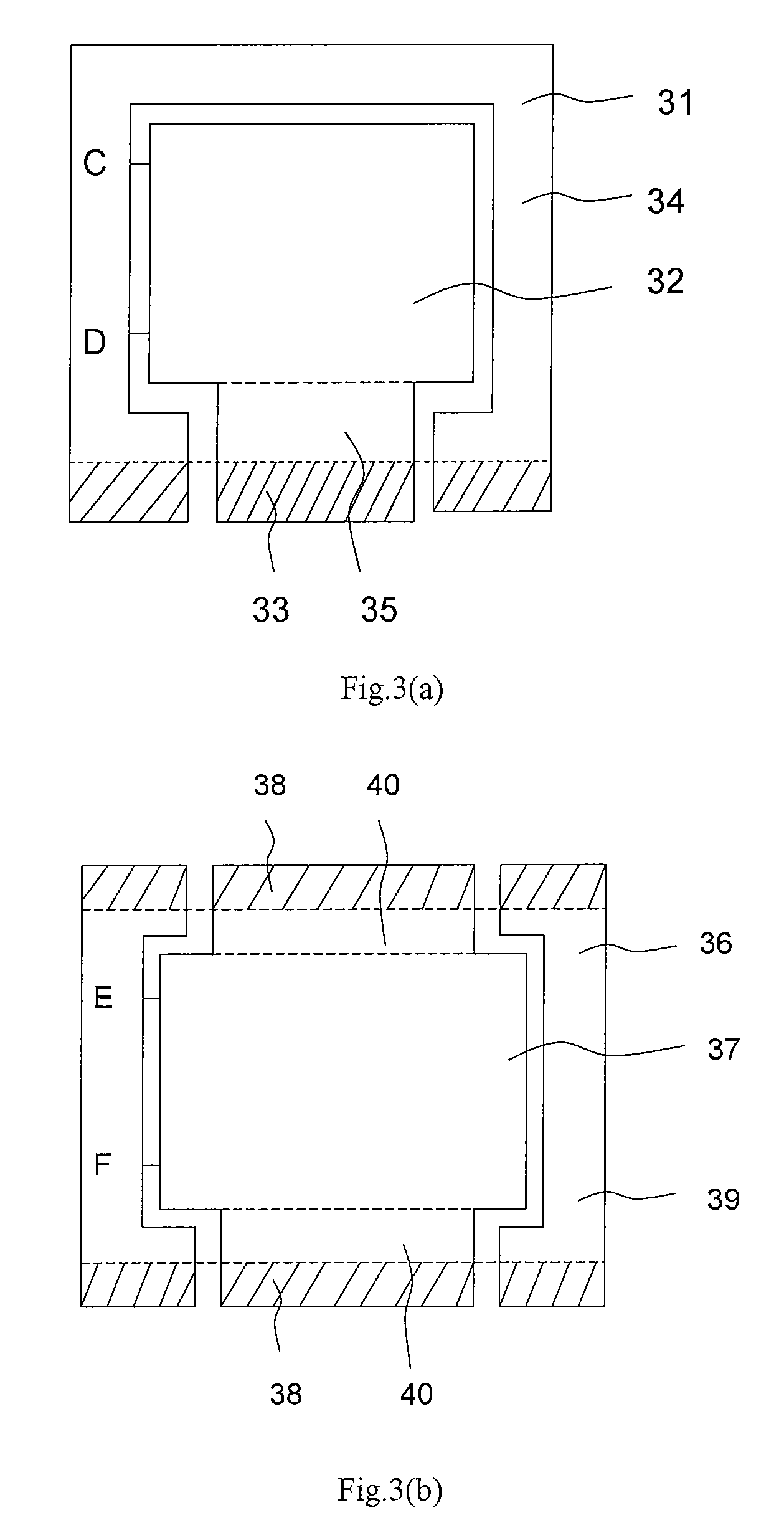
[0043]Turning to FIG. 4(b), it is a structural section diagram of the organic electroluminescent display of Display Example 1, in which the display comprises a substrate 41, an organic electroluminescent device 48, a packaging sheet 44, a packaging region 49, a packaging region and electrode transferring region 42, a bonding region 45, a drying region 47, and in which the organic electroluminescent device 48 is disposed on the substrate 41, the packaging sheet 44 is disposed on the organic electroluminescent device 48, the packaging sheet 44 is connected with the substrate 41 through a packaging adhesive in order to package the device, and a recess is provided in the middle part of the packaging sheet 44 for placing a drying agent. In addition, from the section diagram of the organic electroluminescent device as shown in FIG. 4(b), it can be seen that the packaging region 49, the packaging region and electrode transferring region 42 and bonding region 45 are disposed on the surface ...

example 2

[0046]Turning to FIG. 5, it is a structural section diagram of two surfaces of the organic electroluminescent display of Display Example 2 of the present invention, in which the display comprises a first display device, a second device and a packaging sheet sandwiched between the first display device and the second display device, in which the first display device comprises a first substrate 50 and a first component 51, and correspondingly the second display also comprises a substrate and a second component, and the packaging sheet 52 is sandwiched between the two display devices and has two surfaces which separately are adjacent to the two display devices. The packaging sheet 52 is joined to the first substrate and the second substrate through a packaging adhesive, a recess is disposed at each of the two surfaces of the packaging sheet 52 for placing a drying agent. In addition, a packaging region 55, a packaging region and electrode leads transferring region 53 and bonding region ...

example 3

[0050]The present example relates to an organic electroluminescent while light source, preferably having a device structure as follows:

[0051]substrate / ITO / NPB / NPB:Rubrene / BAlq:TBPe / Alq3 / LiF / Al.

[0052]FIG. 6 shows the schematic diagrams of a procedure for making the light source of the present example, in which the procedure comprises the following steps:

[0053]1) Cleaning and drying a transparent glass substrate, and sputtering a transparent conductive film ITO thereon as anodes of the device, in which the ITO has a square resistance of 5Ω and a film thickness of 100.00 nm;

[0054]2) Placing the above cleaned and dried ITO glass into a vacuum chamber having a pressure of 1×10⁻⁵Pa, vapor depositing on the ITO film a layer of N,N′-bis-(1-naphthyl)-N,N′-biphenyl-(1,1′-diphenyl)-4,4′-diamine (NPB), having a thickness of 100 nm, as the hole transport layer of the device;

[0055]3) Keeping the above vacuum pressure, vapor depositing on the hole transport layer a electroluminescent layer, in whi...


PUM


Abstract

The present invention relates to an organic electroluminescent display, including a substrate, a set of anodes, an organic functional layer, a set of cathodes and a packaging sheet, wherein a set of electrode leads are disposed on the packaging sheet for electrical connection with a control circuit of the display, and the electrode leads includes a set of anode leads and a set of cathode leads which are electrically connected with the corresponding anodes and cathodes on the substrate, respectively. The present invention further relates to a double-sided organic electroluminescent display having the above features.

Description

CROSS-REFERENCE TO RELATED APPLICATIONS[0001]This application claims priority from Chinese Application No. 200710065097.4, filed on Apr. 3, 2007, entitled “Organic Luminous Display,” and Chinese Application No. 200710098872.6, filed on Apr. 28, 2007, entitled “Electroluminescent Light Source,” the contents which are incorporated herein by reference in their entirety.FIELD OF THE INVENTION[0002]The present invention pertains to organic electroluminescent field, especially relates to an organic electroluminescent display and to an organic electroluminescent light source.BACKGROUND OF THE INVENTION[0003]Organic electroluminescent devices have a lot of excellent properties such as self-luminescence, high-brightness, broad view angle, high contrast, low energy consumption, rapid response, broad range of operation temperature, high luminescent efficiency, simple process for manufacture, and so on, so that they arrest many attentions around the world.[0004]Currently, electrode leads of an ...

Claims


Application Information

Patent Timeline
IPC IPC(8): H01J1/62
CPCH01L25/048H01L27/3267H01L27/3276H01L27/3288H01L51/524H01L2924/0002H01L51/5246H01L2924/00H10K59/90H10K59/128H10K59/179H10K59/131H10K50/841H10K50/8426
Inventor QIU, YONGZHANG, SHENFUZHANG, GUOHUIWU, KONGWUGAO, YUDI
Owner TSINGHUA UNIV
Why Eureka
Try Eureka