Eureka AIR delivers breakthrough ideas for toughest innovation challenges, trusted by R&D personnel around the world.

Accumulation field effect microelectronic device and process for the formation thereof

Active Publication Date: 2008-10-16
PENN STATE RES FOUND
View PDF19 Cites 222 Cited by
  • Summary
  • Abstract
  • Description
  • Claims
  • Application Information

AI Technical Summary

Benefits of technology

[0009]A gated microelectronic device is provided that has an ohmic contact to a source semiconductor region characterized by a source dopant type and concentration and linear extent. There is also an ohmic contact to a drain semiconductor region which is characterized by a drain dopant type and concentration and linear extent. A voltage is imposed in operation between the drain and the source. A channel portion intermediate between the source and the drain is characterized by a channel portion dopant type and concentration and defines a channel portion line

Problems solved by technology

Unfortunately, reducing insulating layer thickness beyond a certain point has proven difficult as gate leakage current outweighs any benefits achieved through gate capacitance increases.
Fabricating such small devices can be costly since the processing involved generally necessitates multiple etching and deposition steps all guided by lithography.
The prior art has not taught the role of doping concentration on on-state current, has not taught the importance of the position of ohmic contacts with respect to channel edges, the correct role of C1 in on-state operation, nor the role of the doping concentration in the various regions of the transistor on performance of single doping-type FETs.
The role of the voltage VDS developed between the source and drain in a single doping type structure has not be realized and there has been a lacking of guidance as to device design.
In fact, Mayer et al. has strongly taught away from NW FET structures with single doping type citing that they are not capable of good on-current to off-current ratios nor of good subthreshold slopes (swing) values.8 < / sup
Further, having a FET device whose dependence on gate capacitance is weaker than that of a MOSFET overcomes the problem of the need for close fabrication control of the gate insulator.

Method used


Image

  • Accumulation field effect microelectronic device and process for the formation thereof
  • Accumulation field effect microelectronic device and process for the formation thereof
  • Accumulation field effect microelectronic device and process for the formation thereof

Examples


example 1

AMOSFET Fabricated Using a Template an a Substrate

[0036]An inventive device is fabricated using silicon nanowire material. The nanowires are grown on a substrate and transistors fabricated in situ. No transfer process is utilized. An inventive device fabrication began with the vapor-liquid-solid (VLS), grow-in-place silicon nanowire (SiNW) growth process in growth channels approach previously detained in U.S. Patent Application Publication 2005 / 0176228.

[0037]In the grow-in-place variation used here, Corning 1737 glass, serves as the substrate on which the permanent growth-templates are constructed. Template construction is known2,4 and the use of such templates is summarized in FIG. 3 for the fabrication of the inventive devices of this example. The resulting permanent templates are designed to allow vapor-liquid-solid (VLS) nanowire growth in, and then finally extrusion out of, the guiding nanochannels under the capping layer of FIG. 3 in the particular version of grow-in-place use...

example 2

Growth Channel Template Transfer and Stamp Technique

[0041]The growth channel template method utilized with a transfer approach is detailed for also producing an inventive device. FIGS. 4A-D and FIGS. 5A-D show the schematic representations of the use of the growth channel templates with a transfer approach. These growth channel templates are made on a mother substrate. Two versions of channel templates are shown: a long / encapsulated channel template (FIG. 4) and a short channel template (FIG. 5). These both show the channel template transfer after nanowire growth from a mother substrate to a flexible substrate. Inventive device fabrication is completed either before or after transfer. Growth channel templates can also be transferred from the mother substrate to the final substrate before nanowire, nanoribbon or nanotube growth in the same way. When done in this manner, full transistor fabrication is done after wire / ribbon growth transfer, with nanowire, nanoribbon or nanotube growth...

example 3

Thin Film Transistor Fabrication

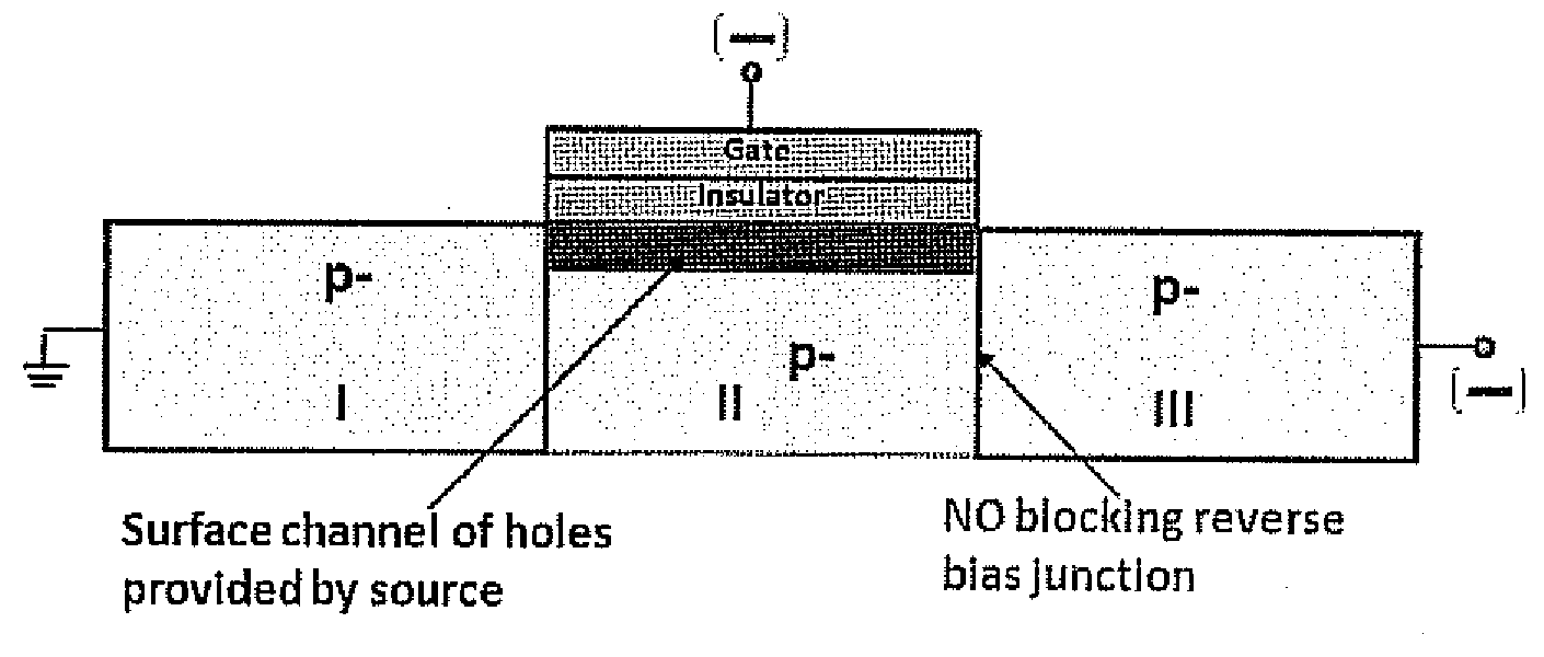
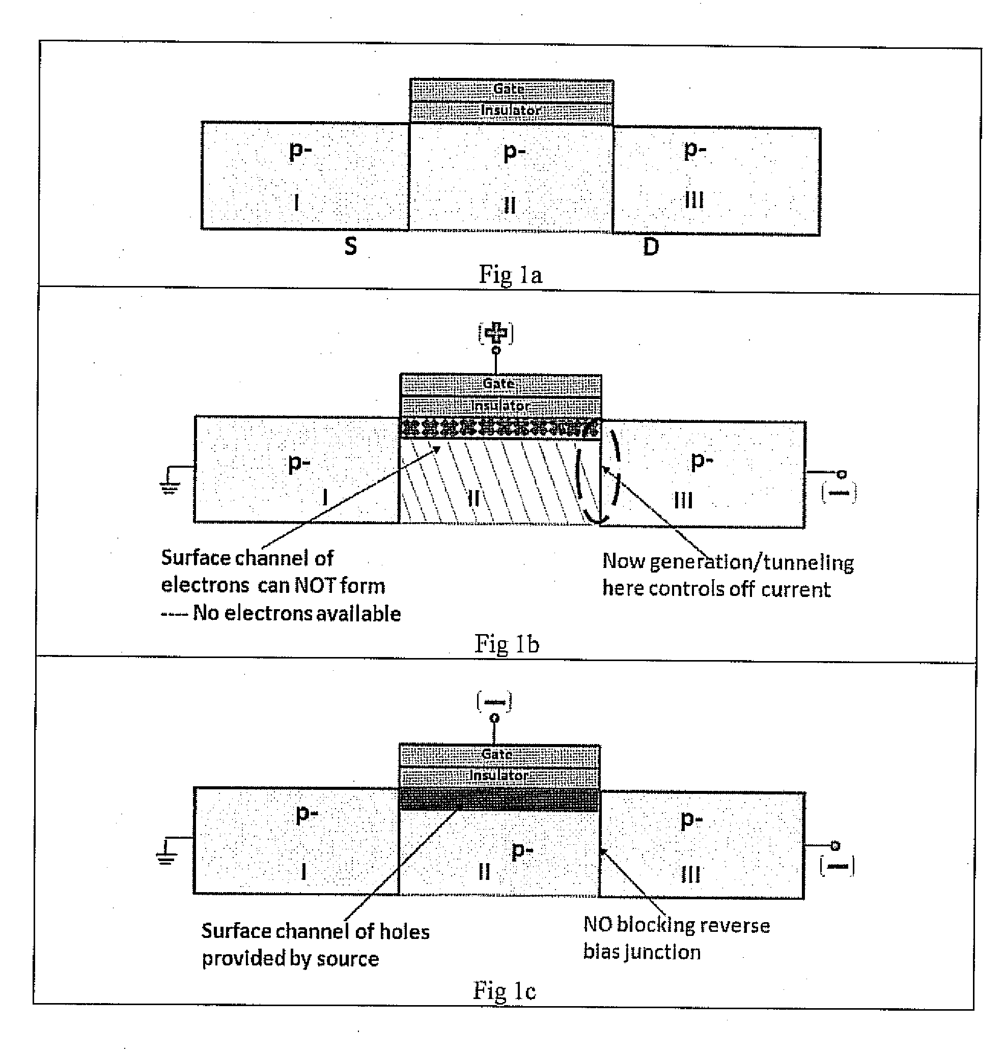
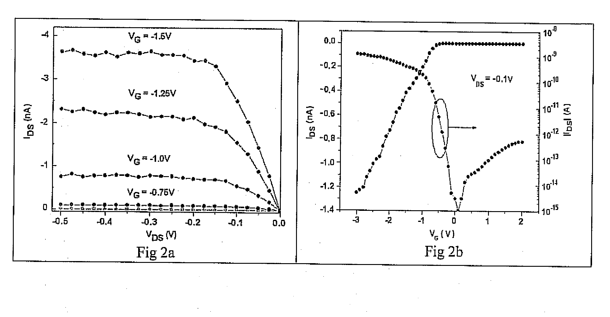
[0042]As discussed above, an inventive device can be fabricated using ultra thin film semiconductors. These are deposited and defined, for example, by etching or are grown nanoribbons produced, for example, by the previously discussed VLS grown-in-place method. Unlike conventional TFT transitors, AMOSFETs fabricated with thin film semiconductors use films of only one doping type (and not n / i / n or p / i / p dopings) and the doping concentration is crucial in determining the on-current magnitude. As is also characteristic of AMOSFET devices, the on-current is not proportional to gate capacitance and gate insulator thickness control need not be of paramount concern.


PUM


Abstract

A gated microelectronic device is provided that has a source with a source ohmic contact with the source characterized by a source dopant type and concentration. A drain with a drain ohmic contact with the drain characterized by a drain dopant type and concentration. An intermediate channel portion characterized by a channel portion dopant type and concentration. An insulative dielectric is in contact with the channel portion and overlaid in turn by a gate. A gate contact applies a gate voltage bias to control charge carrier accumulation and depletion in the underlying channel portion. This channel portion has a dimension normal to the gate which is fully depleted in the off-state. The dopant type is the same across the source, drain and the channel portion of the device. The device on-state current is determined by the doping and, unlike a MOSFET, is not directly proportional to device capacitance.

Description

RELATED APPLICATIONS[0001]This application is a non-provisional application that claims priority benefit of U.S. Provisional Application Ser. No. 60 / 911,378 filed 12 Apr. 2007 and U.S. Provisional Application Ser. No. 60 / 951,547 filed 24 Jul. 2007; the contents of which are incorporated herein by reference.FIELD OF THE INVENTION[0002]The present invention relates in general to field effect microelectronic devices and in particular to a field effect device having a substantially single dopant type across source, gated intermediate portion, and drain.BACKGROUND OF THE INVENTION[0003]A conventional metal oxide semiconductor field effect transistor (MOSFET) utilizes heavily doped source and drain semiconductor regions to form ohmic contacts to a gate induced inversion-layer channel portion. In the on-state, transport in this channel portion controls the source-drain current, IDS. In the on-state, the inverted channel is not shunted due to the presence of a reversed-biased n / p or p / n jun...

Claims


Application Information

Patent Timeline
IPC IPC(8): H01L29/00H01L21/336
CPCB82Y10/00H01L29/0665H01L29/0673H01L29/78603H01L29/78618H01L29/78672H01L29/78681H01L29/78684H01L29/7869H01L29/78696
Inventor FONASH, STEPHEN J.SHAN, YINGHUIASHOK, S.
Owner PENN STATE RES FOUND
Why Eureka
Eureka Blog
Learn More