
Etching method and semiconductor device fabrication method

a fabrication method and semiconductor technology, applied in the direction of electrical equipment, basic electric elements, electric discharge tubes, etc., can solve the problems of difficult or impossible for a semiconductor device to have a desired performance, and achieve the effect of increasing the selectivity of a polysilicon film and preventing the formation of recesses

Inactive Publication Date: 2008-10-23
TOKYO ELECTRON LTD
View PDF5 Cites 3 Cited by
  • Summary
  • Abstract
  • Description
  • Claims
  • Application Information

AI Technical Summary

Benefits of technology

[0010]The present invention provides etching method and semiconductor device fabrication method that are capable of increasing the selectivity of a polysilicon film to a silicon oxide film and preventing recesses from being formed on a silicon base layer.
[0012]With the etching method according to the first aspect of this invention, the polysilicon film is etched such that a part of the polysilicon film remains on the silicon oxide film, and then the part of the polysilicon film remaining on the silicon oxide film is etched at an ambient pressure of 33.3 Pa to 93.3 Pa using plasma generated from a processing gas not containing oxygen gas. At a pressure equal to or higher than 33.3 Pa, the sputter ability of plasma is lowered, and the etch rate of the oxide film is greatly lowered than that of the polysilicon film, which makes it possible to increase the selectivity of the polysilicon film to the silicon oxide film. Since oxygen gas is not used, the silicon base layer beneath the silicon oxide film is not oxidized, which makes it possible to suppress recesses from being formed on the silicon base layer.
[0013]In the second etching step, the part of the polysilicon film remaining on the silicon oxide film can be etched at an ambient pressure of 40.0 Pa to 80.0 Pa. In this case, the unetched part of the polysilicon film is etched at an ambient pressure of 40.0 Pa to 80.0 Pa. At a pressure equal to or higher than 40.0 Pa, the sputter ability of plasma is extremely weakened, and an increased selectivity of the polysilicon film to the silicon oxide film can be ensured. As a result, occurrences of cracks on the silicon oxide film and the like can be prevented.
[0015]In that case, the processing gas is a mixture of hydrobromic gas and inactive gas. Using plasma generated from the hydrobromic gas, the polysilicon film can be efficiently etched, to thereby improve throughput.
[0017]In that case, the polysilicon film is etched in the first etching step using plasma generated from hydrobromic gas, fluorocarbon gas, or chlorine gas. Plasma generated from the hydrobromic gas or the fluorocarbon gas or the chlorine gas can efficiently etch the polysilicon film, thereby further improve throughput.
[0021]With the semiconductor device fabrication method according to the second aspect of this invention, the selectivity of the polysilicon film to the silicon oxide film can be increased and recess formation can be suppressed, as in the etching method according to the first aspect.

Problems solved by technology

This makes it difficult or impossible for a semiconductor device to have a desired performance.

Method used


Image

  • Etching method and semiconductor device fabrication method
  • Etching method and semiconductor device fabrication method
  • Etching method and semiconductor device fabrication method

Examples


example i

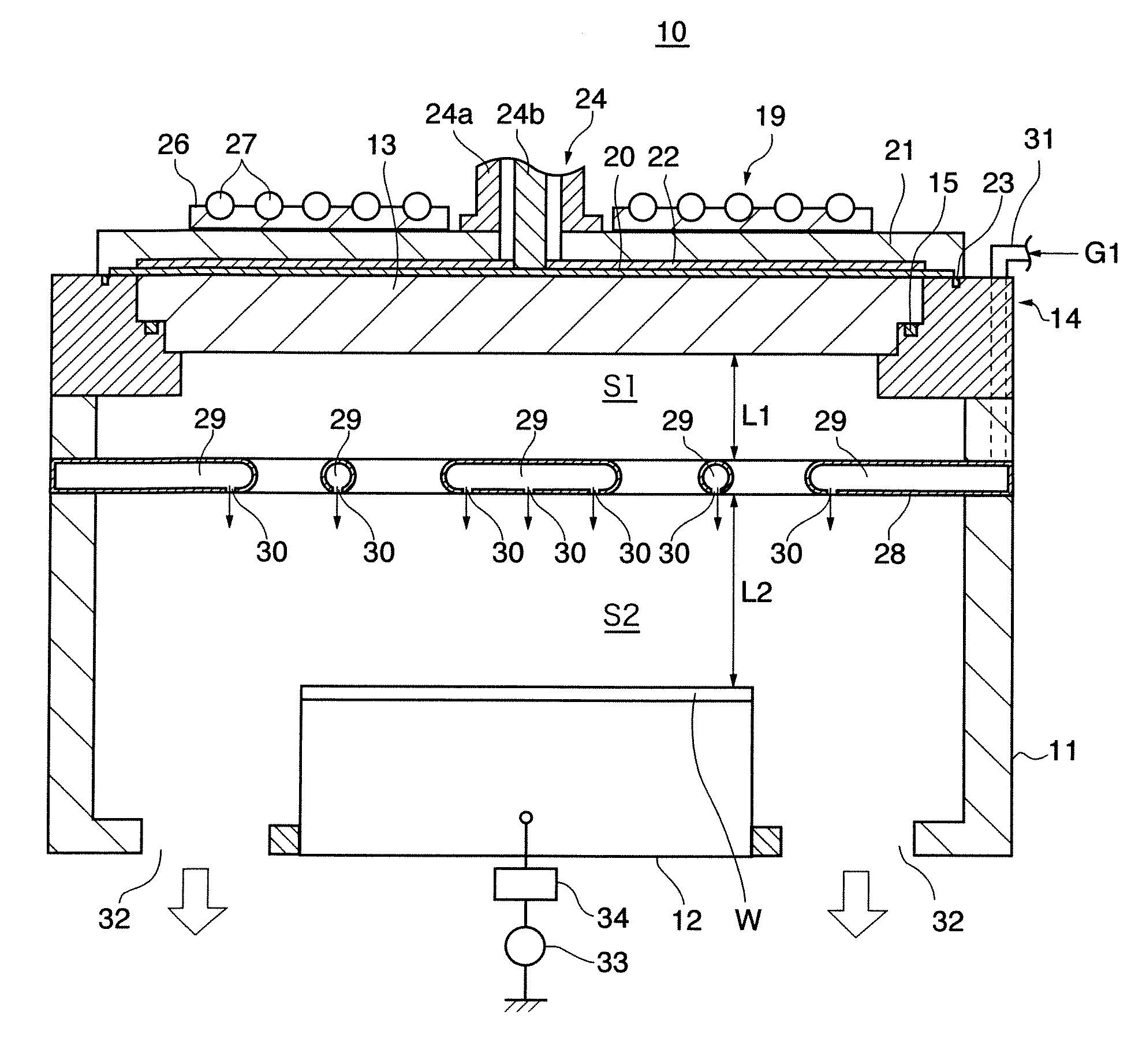
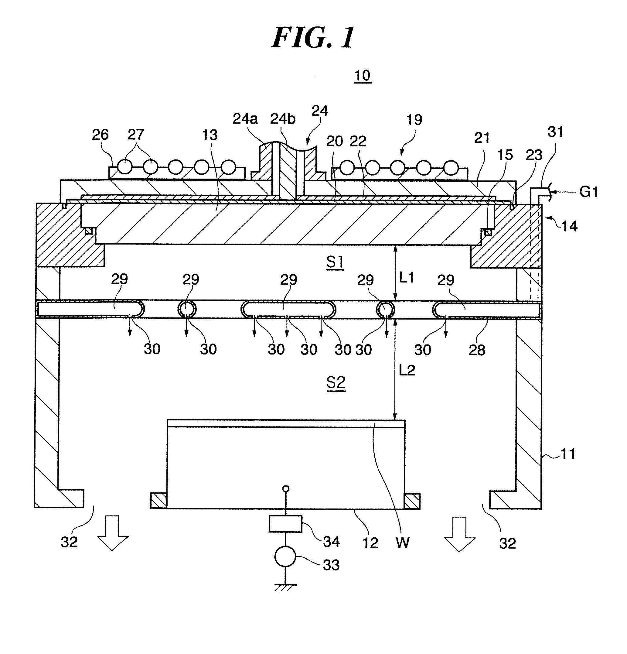
[0080]A wafer W shown in FIG. 4 was prepared and transferred into the processing vessel 11 of the substrate processing apparatus 10. HBr gas, O2 gas, and Ar gas were supplied as the processing gas G1 into the processing space S2. The pressure in the processing spaces S1, S2 was set at 4.0 Pa, a microwave of 2.45 GHz was supplied to the radial line slot antenna 19, and high frequency power of 400 KHz was supplied to the susceptor 12, whereby the part of the polysilicon film 37 exposed through the opening 40 was etched to an extent that such film part slightly remained on the gate oxide film 36. Then HBr gas and He gas were supplied to the processing space S2, and the pressure in the processing spaces S1, S2 was set at 66.7 Pa. Using plasma generated from the HBr gas and the like, the residue polysilicon film was etched. It was confirmed that the residue polysilicon film was completely removed but the gate oxide film 36 was hardly etched.

[0081]Then the wafer W was transferred into a p...

example 2

[0087]Under the same conditions as in Example 1, the part of the polysilicon film 37 exposed through the opening 40 was etched so as to slightly remain on the gate oxide film 36. Then, the residue polysilicon film was etched under the same conditions as in Example 1 except that the pressure in the processing spaces S1, S2 was set at 33.3 Pa.

[0088]Then, the gate oxide film 36 exposed due to complete removal of the residue polysilicon film was removed, and then the anti-reflection film 38 and the resist film 39 were removed. Based on subsequent observations on the gate formed on the wafer W, it was confirmed that, although there were a few recesses on the silicon base layer 35, the depths of the recesses were less than a critical depth below which there is no affection to ion implantation to the silicon base layer 35 (refer to FIG. 7(A)). It was also confirmed that the gate oxide film 36 in the gate was not formed into a shape widened toward its end.

example 3

[0089]Under the same conditions as in Example 1, the part of the polysilicon film 37 exposed through the opening 40 was etched so as to slightly remain on the gate oxide film 36. Then, the residue polysilicon film was etched under the same conditions as in Example 1 except that the pressure in the processing spaces S1, S2 was set at 93.3 Pa (700 mTorr).

[0090]Then, the gate oxide film 36 exposed due to complete removal of the residue polysilicon film was removed. In succession, the anti-reflection film 38 and the resist film 39 were removed, and subsequently the gate formed on the wafer W was observed. As a result, it was confirmed that there were no recesses on the silicon base layer 35 and that the gate oxide film 36 in the gate was formed into a shape widened toward an end thereof, but the magnitude of being widened is less than a critical magnitude below which there is no affection to ion implantation to the silicon base layer 35 (FIG. 7B).

[0091]It should be noted that in Example...


PUM


Abstract

An etching method capable of increasing the selectivity of a polysilicon film to a silicon oxide film and suppressing recess formation on a silicon base layer. That part of the polysilicon film of a wafer transferred into a processing vessel which is exposed through an opening is etched so as to slightly remain on a gate oxide film. The pressure in a processing space is set to 66.7 Pa, HBr gas and He gas are supplied to the processing space, and a microwave of 2.45 GHz is supplied to a radial line slot antenna. The polysilicon film is etched by plasma generated from the HBr gas so as to be completely removed, the exposed gate oxide film is etched, and a resist film and an anti-reflection film are etched.

Description

BACKGROUND OF THE INVENTION[0001]1. Field of the Invention[0002]The present invention relates to an etching method and a semiconductor device fabrication method, and more particularly, to an etching method for etching a polysilicon layer formed on a gate oxide film and a semiconductor device fabrication method in which the etching method is implemented.[0003]2. Description of the Related Art[0004]For formation of a semiconductor device gate of a single layer of polysilicon (polycrystal silicon), a wafer is processed that has a silicon base layer 100 on which are formed in layers a gate oxide film 101 of silicon oxide, a polysilicon film 102, an anti-reflection film (a BARC film) 103, and a resist film 104 (see, FIG. 8A). In this wafer, the anti-reflection film 103 and the resist film 104 are formed in predetermined patterns and an opening 105 through which the polysilicon film 102 is exposed is formed at a predetermined location on the wafer.[0005]A wafer processing process includes...

Claims


Application Information

Patent Timeline
IPC IPC(8): H01L21/302
CPCH01L21/32137H01J37/32192H01L21/3065
Inventor IIJIMA, ETSUOHORIGUCHI, KATSUMI
Owner TOKYO ELECTRON LTD
Learn More