Composition and Method for Recycling Semiconductor Wafers Having Low-K Dielectric Materials Thereon

a technology of dielectric materials and semiconductor wafers, applied in the field of composition and method for recycling semiconductor wafers having low-k dielectric materials thereon, can solve the problems of non-uniform deposition of cdo layer, processing problems, and significant non-productive cos

Active Publication Date: 2008-10-23
ENTEGRIS INC
View PDF61 Cites 86 Cited by
  • Summary
  • Abstract
  • Description
  • Claims
  • Application Information

AI Technical Summary

Benefits of technology

[0011]The present invention relates to compositions and processes useful for the removal of low-k dielectric and other material layers, including carbon doped oxide material layers, from a rejected microelectronic device structure having said material deposited thereon, for recycling and / or reuse of said microelectronic device structure, and methods of using such compositions and products or intermediate products manufactured using the same.

Problems solved by technology

Any number of processing problems may occur, for example, the non-uniform deposition of the CDO layer or a subsequent etching error.
A number of quality control testing methods are performed following selected processing steps whereby the acceptability of the semiconductor wafer may be rejected and “scrapped” for various reasons resulting in a significant non-productive cost.
As semiconductor wafer manufacturing moves to larger diameter wafers, for example 12 inch wafers, scrapping and recycling a process wafer off-site becomes increasingly more unattractive because of the high non-productive cost.
For example, high fluoride concentrations and high organic solvent concentrations may make a composition difficult to use in high volume manufacturing due to wastewater disposal issues.
Depending on the level of chemical oxygen demand (COD) of the formulation, whereby the COD of a solution is a measure of the amount of organic compounds that can be fully oxidized to carbon dioxide in the presence of a strong oxidant under acidic conditions, the formulation may not be allowed in the facility wastewater for direct return to the environment.
Disadvantageously, incineration systems may not accept wastewater samples containing high fluoride concentrations because the fluoride source may damage the incinerator materials of construction.

Method used


Image

  • Composition and Method for Recycling Semiconductor Wafers Having Low-K Dielectric Materials Thereon
  • Composition and Method for Recycling Semiconductor Wafers Having Low-K Dielectric Materials Thereon
  • Composition and Method for Recycling Semiconductor Wafers Having Low-K Dielectric Materials Thereon

Examples


example 1

[0129]The pH of Formulation A diluted 20:1 with DI water was determined to be 3.2.

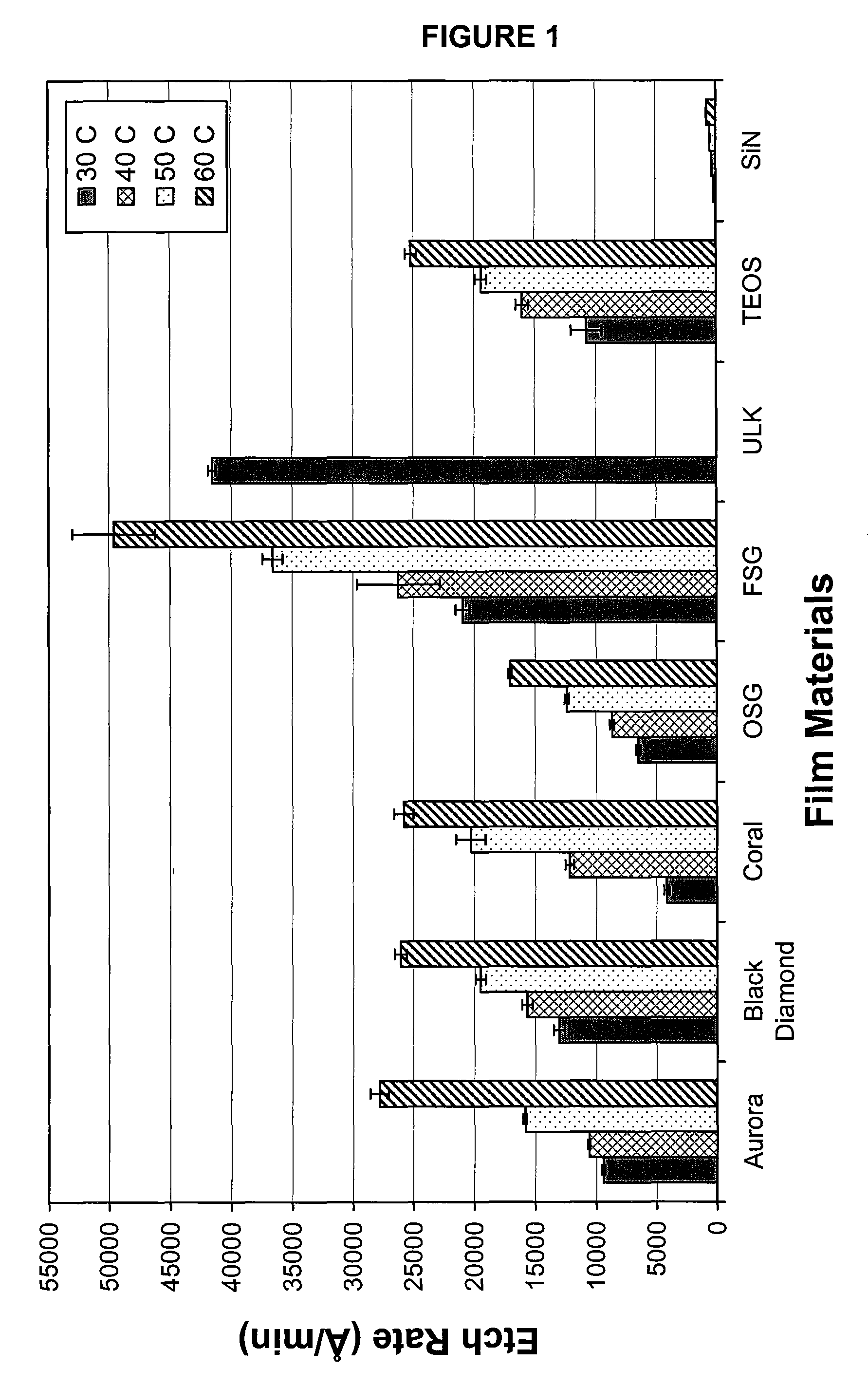
[0130]Bare Si substrates having blanketed BD materials thereon were statically soaked in concentrated Formulation A for 2 min to 5 min at 40° C. to 60° C. as indicated in Table 1. The BD material layers were characterized by the method of depositing the BLACK DIAMOND™ material as well as the thickness of the BD layers. The first bare Si substrate had a blanketed BLACK DIAMOND™ layer deposited using the proprietary BLACK DIAMOND™ process and had a thickness of approximately 6,500 Å (hereinafter BDTM). The second bare Si substrate had a blanketed BD derivative material deposited using a proprietary deposition process and had a thickness of approximately 13,000 Å (hereinafter BDD1). The third bare Si substrate had a blanketed BD derivative material deposited using another proprietary deposition process and had a thickness of approximately 12,000 Å (hereinafter BDD2).

[0131]The results of the static soak ar...

example 2

[0133]Blanketed polysilicon was statically soaked in Formulation A for 30 minutes at various temperatures and the etch rate of the polysilicon determined. The results are summarized in Table 2 hereinbelow.

TABLE 2Results of static soak of polysilicon in Formulation A.PolySi etchtemperature / ° C.rate / Å min−1401.1501.4601.7

[0134]It can be seen that the etch rate of polysilicon in Formulation A was negligible in the temperature range studied herein at extreme soaking conditions, e.g., a soak for 30 minutes. This suggests that Formulation A will not damage the underlying polysilicon material.

example 3

[0135]Samples of bare silicon, BDTM, BDD1, and BDD2 were statically soaked in Formulation A for 200 minutes at 60° C. to mimic extreme soaking conditions. Following immersion for the specified time, the samples were removed from the static soak bath, rinsed, dried and the Atomic Force Microscopic (AFM) surface roughness determined. The results are reported in Table 3 hereinbelow.

TABLE 3Results of static soak of bare Si and BD materials in Formulation A.Formulation Acontrolbare SiBDTMbare Si (nm)(nm)(nm)BDD1 (nm)BDD2 (nm)1 m scan0.1740.4020.3360.4050.3805 m scan0.1450.6880.2960.5710.503

[0136]It can be seen that the bare Si substrate was not significantly damaged during the extreme soak of the respective substrates in Formulation A. For example, the largest numerical change from 0.145 nm to 0.688 nm equates to negligible damage to the surface of the bare Si surface. These results suggest that Formulation A will not damage the underlying bare Si substrate either.


PUM

PropertyMeasurementUnit
dielectric constantaaaaaaaaaa
CODaaaaaaaaaa
CODaaaaaaaaaa

Abstract

A removal composition and process for removing low-k dielectric material, etch stop material, and/or metal stack material from a rejected microelectronic device structure having same thereon. The removal composition includes hydrofluoric acid. The composition achieves at least partial removal of the material(s) from the surface of the microelectronic device structure having same thereon, for recycling and/or reuse of said structure, without damage to the underlying polysilicon or bare silicon layer employed in the semiconductor architecture.

Description

FIELD OF THE INVENTION[0001]The present invention relates to compositions and processes useful for the removal of low-k dielectric and other material layers from a rejected substrate or article having said material deposited thereon, for recycling / reworking and / or reuse of said substrate or article, and to products manufactured using same.DESCRIPTION OF THE RELATED ART[0002]The escalating requirements for performance associated with high density, ultra large scale integration (ULSI) semiconductor wiring have increasingly required the use of low dielectric constant (low-k) insulating layers to increase signal transport speeds as device sizes have decreased.[0003]Typical low-k materials include carbon doped oxides (CDO) deposited using commercially available precursors such as SiLK™, AURORA™, CORAL™, or BLACK DIAMOND™, for example using the proprietary BLACK DIAMOND™ process. Such CDO's are typically formed using chemical vapor deposition (CVD) processes from organosilane and organosi...

Claims


Application Information

Patent Timeline
Patent Type & Authority Applications(United States)
IPC IPC(8): G03F7/42C11D7/32
CPCH01L21/02079H01L21/31111H01L21/32134C09K13/08H01L21/02032H01L21/461
Inventor VISINTIN, PAMELA M.JIANG, PINGKORZENSKI, MICHAEL B.KING, MACKENZIE
Owner ENTEGRIS INC
Why Eureka
Try Eureka