Method of forming oxide-based nano-structured material

a nano-structured material and oxide-based technology, applied in the direction of niobium compounds, chromium oxides/hydrates, liquid/solution decomposition chemical coatings, etc., can solve the problems of high manufacturing cost, large-scale equipment, and complicated conventional method of forming oxide-based nano-structured materials, etc., to achieve excellent crystalline properties, low manufacturing cost, and simple process

Inactive Publication Date: 2008-10-30
ELECTRONICS & TELECOMM RES INST
View PDF5 Cites 2 Cited by
  • Summary
  • Abstract
  • Description
  • Claims
  • Application Information

AI Technical Summary

Benefits of technology

[0021]According to a method of forming an oxide-based nano-structured material of the present invention, the nano-structured material does not include an impurity since the oxide-based nano-structured material is grown using a nano-nucleus having the same composition as the desired oxide-based nano-structured material. Further, an oxide-based nano-structured material having excellent crystalline properties can be formed through a simple process at low manufacturing costs by (employing a wet chemical process to form the nano-nucleus. Therefore, the oxide-based nano-structured material formed according to the present invention can provide a uniform connection when applied to minimized and integrated electronic circuits, and also provide stable electrical and optical properties.

Problems solved by technology

However, this conventional method of forming an oxide-based nano-structured material is complicated and requires a large area substrate, and thus also requires large-scale equipment for the growth of the oxide-based nano-structured material.
Further, as a result of the complicated process of forming the noble metal nano particles which function as the nucleus, and then growing the oxide-based nano-structured material therefrom, the noble metal remains in the resulting oxide-based nano-structured material as an impurity.
In addition, the manufacturing costs increase due to the noble metal.
Therefore, mass production of the oxide-based nano-structured material is limited.
In addition, a connection between the noble metal particles or the noble metal cluster and the oxide-based nano-structured material is incomplete since they have different compositions, and a dopant is not easily injected into the resulting nano-structure.
In particular, although the material itself used in the nano-structured material has excellent electrical properties, it is not easy to control growth rate, size, and shape of the nano-structured material according to a plane index of the noble metal used as the nucleus.
Thus, the oxide-based nano-structured material cannot have a uniform composition, shape and size, and as such is unable to have stable properties.
Therefore, since the oxide-based nano-structured material formed according to the conventional method provides unstable electrical properties, application to integrated high-speed electronic circuits is limited.

Method used


Image

  • Method of forming oxide-based nano-structured material
  • Method of forming oxide-based nano-structured material

Examples


Embodiment Construction

[0024]Hereinafter, the present invention will now be described more fully with reference to the accompanying drawing, in which exemplary embodiments of the invention are shown. The invention may, however, be embodied in many different forms and should not be construed as being limited to the embodiments set forth herein; rather, these embodiments are provided so that this disclosure will be thorough and complete, and will fully convey the concept of the invention to those skilled in the art.

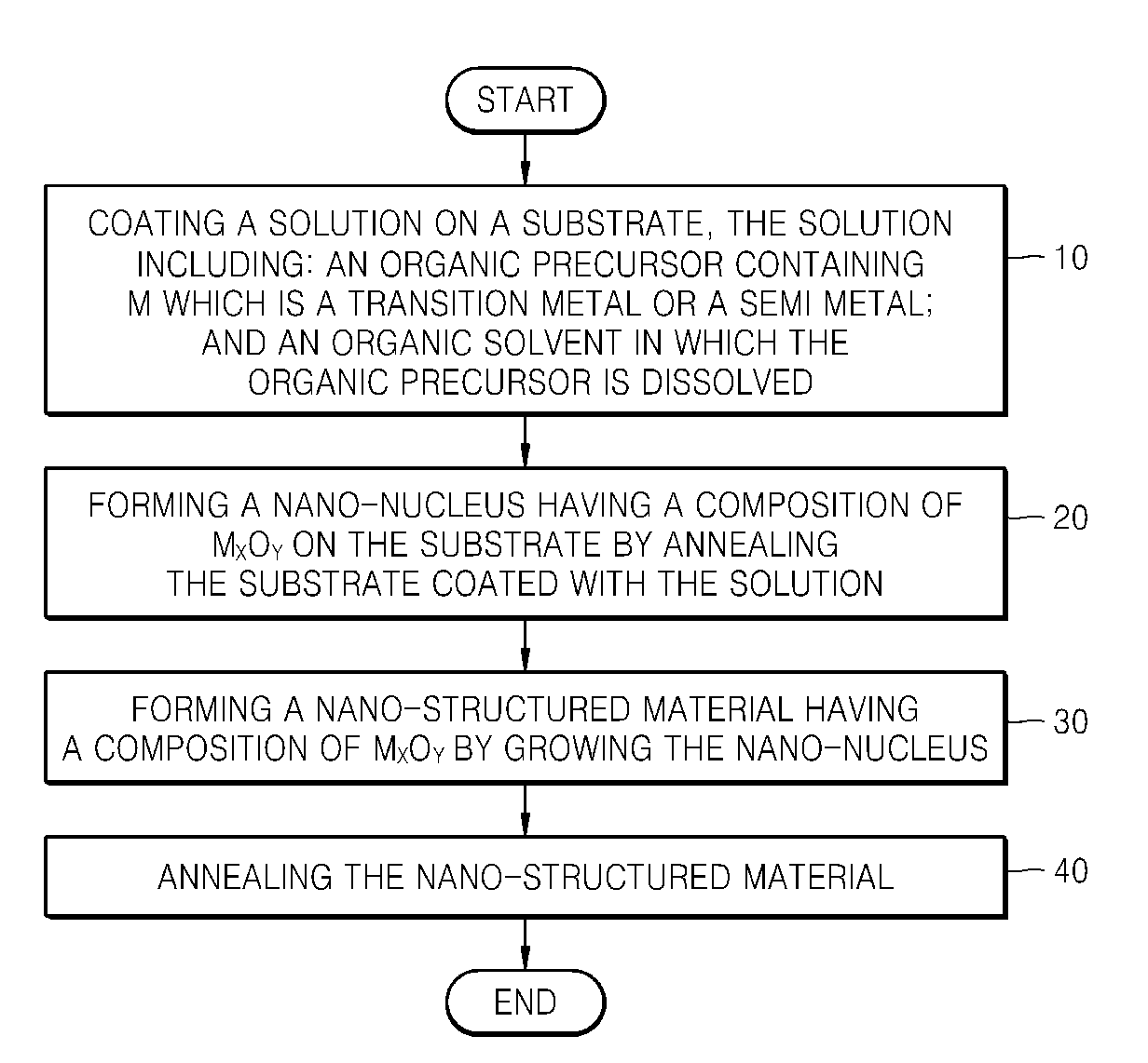
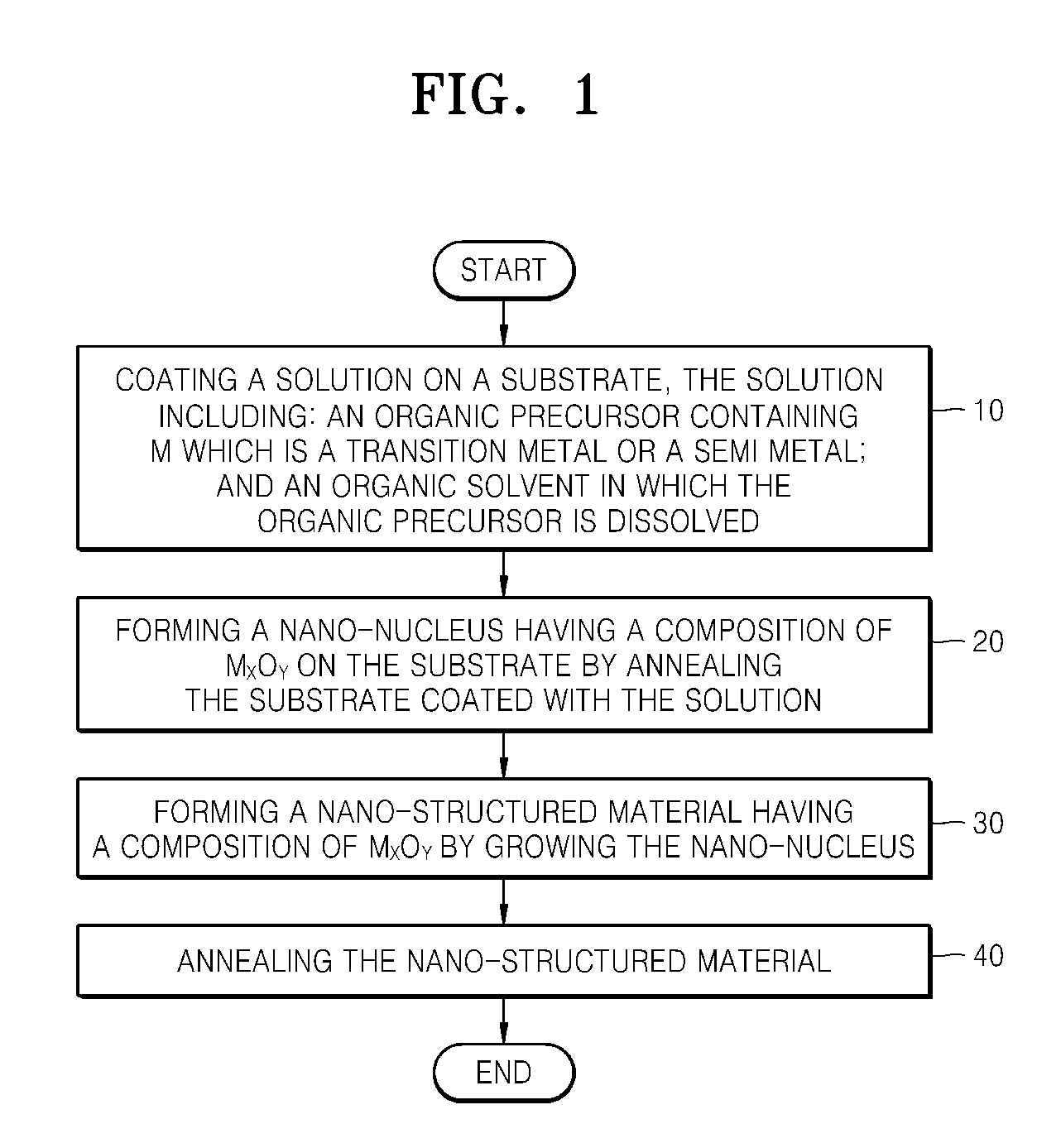
[0025]FIG. 1 is a flow chart illustrating a method of forming an oxide-based nano-structured material according to an embodiment of the present invention.

[0026]Referring to FIG. 1, in operation 10, a solution is coated on a substrate, the solution including: an organic precursor containing M which is a transition metal or a semi metal; and an organic solvent in which the organic precursor is dissolved.

[0027]For this, an organic precursor containing M is mixed with an organic solvent to prepare th...


PUM

PropertyMeasurementUnit
temperatureaaaaaaaaaa
timeaaaaaaaaaa
temperatureaaaaaaaaaa

Abstract

Provided is a method of forming an oxide-based nano-structured material including growing a nano-structured material using a nano-nucleus having the same composition as the desired oxide-based nano-structured material. A solution is coated on a substrate, the solution including: an organic precursor containing M which is a transition metal or a semi metal; and an organic solvent in which the organic precursor is dissolved. A nano-nucleus having a composition of MxOy is formed on the substrate by annealing the substrate. A nano-structured material having a composition of MxOy is formed by growing the nano-nucleus while supplying a reaction precursor containing M into the nano-nucleus, and the nano-structured material is annealed.

Description

CROSS-REFERENCE TO RELATED PATENT APPLICATION[0001]This application claims the benefit of Korean Patent Application Nos. 10-2006-0122630, filed on Dec. 5, 2006, and 10-2007-0036582, filed on Apr. 13, 2007, in the Korean Intellectual Property Office, the disclosures of which are incorporated herein in their entirety by reference.BACKGROUND OF THE INVENTION[0002]1. Field of the Invention[0003]The present invention relates to a method of forming an oxide-based nano-structured material, and more particularly, to a method of forming a nano-structured material using an oxide of a transition metal or a semi metal.[0004]2. Description of the Related Art[0005]Oxide-based nano-structured materials containing a metal or non-metal element are potentially applicable to the field of nano-electronic devices such as field effect transistors (FETs), single electron transistors (SETs), photodiodes, biochemical sensors, and logic circuits. Accordingly, research on properties of nano-structured materia...

Claims


Application Information

Patent Timeline
Patent Type & Authority Applications(United States)
IPC IPC(8): H01L21/469
CPCB82Y30/00C01G9/02C01G17/02C01G23/047C01G23/053C01G25/02C01G28/02C01G31/02C01G33/00C01G37/02C01P2004/64C23C18/1216C23C18/1245C23C18/1254C23C18/1295B82B3/00B82B1/00B82Y40/00
Inventor KIM, SANG HYEOBLEE, SUN YOUNGMAENG, SUNG LYULMYOUNG, HEY JIN
Owner ELECTRONICS & TELECOMM RES INST
Why Eureka
Try Eureka