Mems Nanoindenter

a nano-indentation device and nano-indentation technology, applied in the direction of instruments, force/torque/work measurement apparatus, paper/cardboard containers, etc., can solve the problems of difficult to perform one type of measurement at a time, large volume of available instruments,

Active Publication Date: 2008-11-13
FEI CO
View PDF5 Cites 18 Cited by
  • Summary
  • Abstract
  • Description
  • Claims
  • Application Information

AI Technical Summary

Benefits of technology

[0018]A force acting on a probe attached to the probe holding structure may be measured by detecting capacitive changes between the membrane and the detect

Problems solved by technology

Instrumentation are available that enable such experiments where an object of interest is tested on the nano scale; however, the available instrumentation is quite large in volume and can only perform one type of measurement at a time due to this.
It is not an easy task with the current state of the art to do nanoindentation measurements on very small structures such as nanotubes.
However, it is very difficult to do nanoindentation experiments in situ of an electron microscope.

Method used


Image

  • Mems Nanoindenter
  • Mems Nanoindenter
  • Mems Nanoindenter

Examples


Embodiment Construction

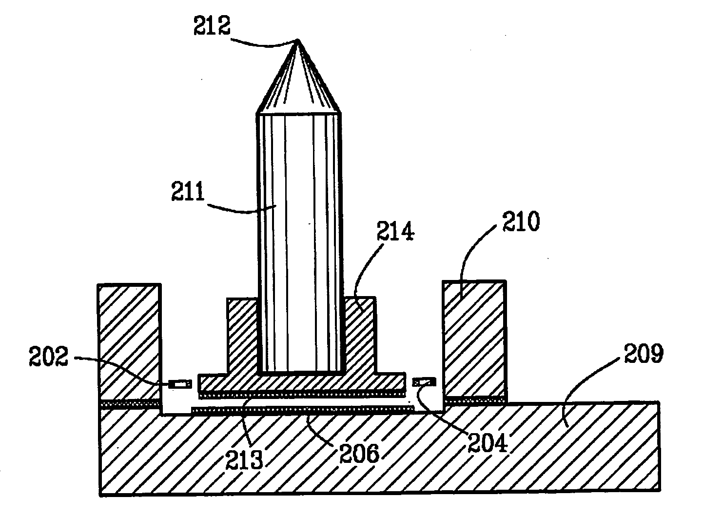
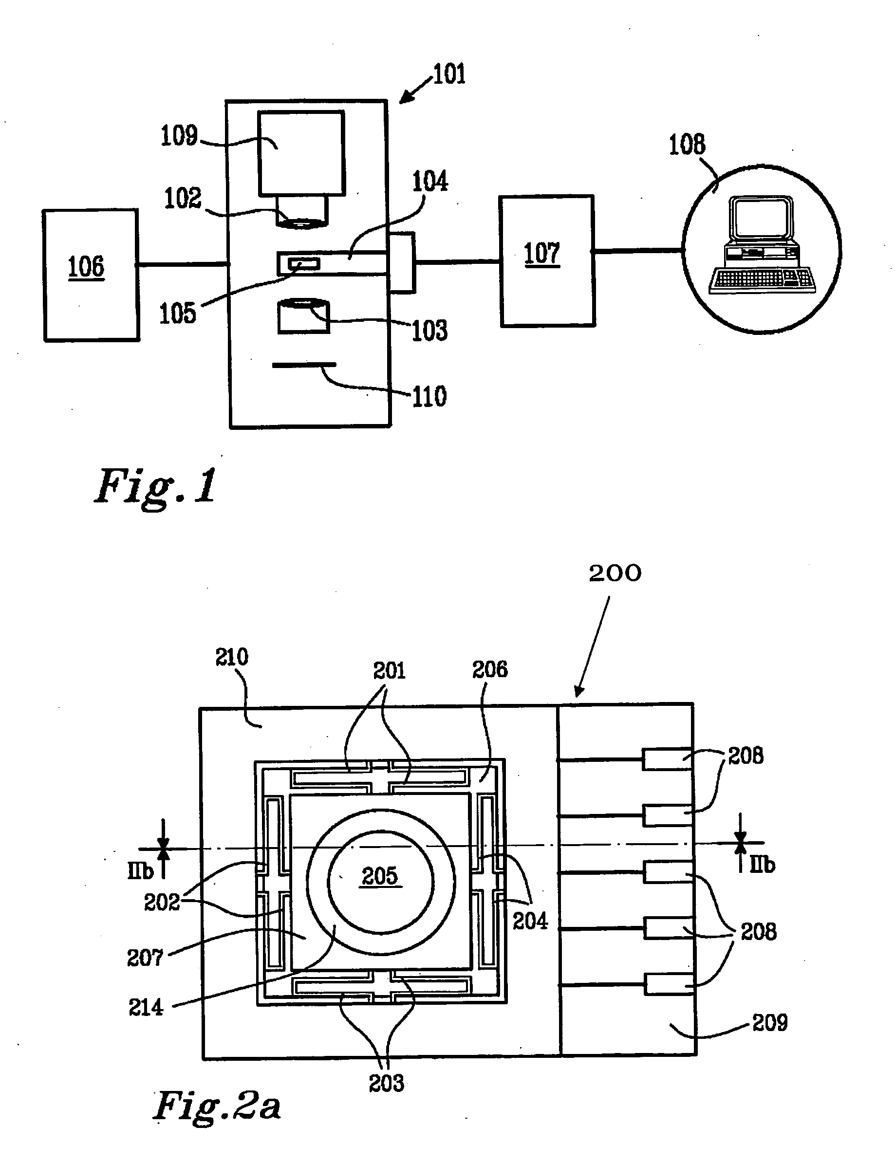
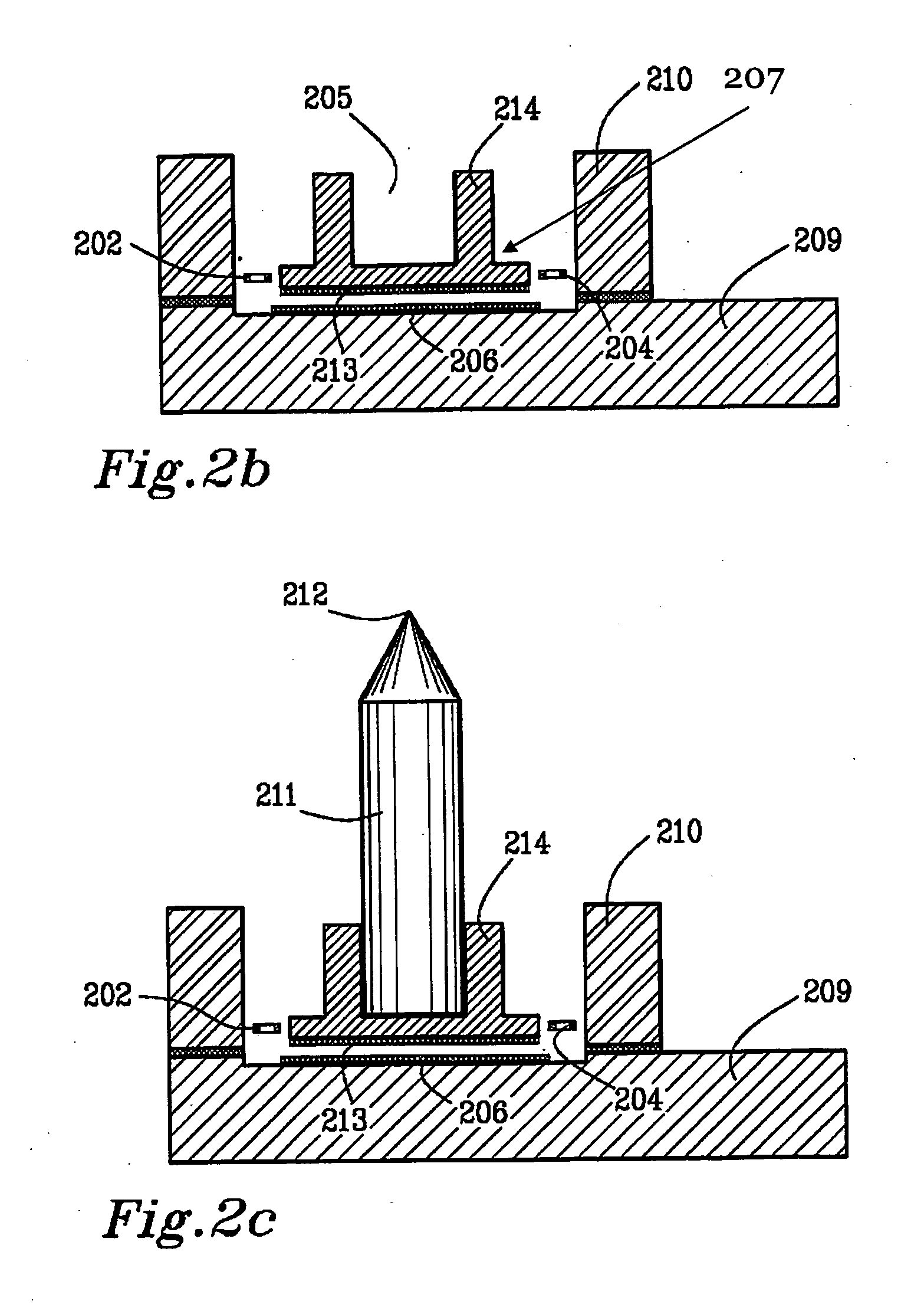
[0051]FIG. 1 illustrates a schematic of an experimental setup system according to the present invention. In a preferred embodiment of the present invention a nanoindenter 105 is provided for a transmission electron microscope (TEM) 101. The nanoindenter is mounted on a TEM sample holder 104 and movement and measurement data is acquired using a measurement system comprising control electronics 107 and a computational system 108 comprising e.g. a personal computer, display unit and interface peripherals (such as a keyboard and mouse).

[0052]The TEM 101 operates by forming a beam of electrons directed towards a sample and after interaction with the sample, the electron beam is directed towards an image viewing or collecting device 110, respectively using magnetic lenses 102 and 103. The electron beam is produced using an electron emitting device 109. The TEM 101 is controlled by a TEM control system 106 as understood by the person skilled in the art. However, it is possible to combine t...


PUM

PropertyMeasurementUnit
Forceaaaaaaaaaa
Dimensionaaaaaaaaaa
Sensitivityaaaaaaaaaa

Abstract

In recent years there has been a growing market for more universal analysis instruments. Analysis tools such as AFM1, TEM2 and nanoindentation work in similar environments. It is therefore possible, within limits, to use the same equipment to do all of these analyses. Conducting nanoindentation experiments in a TEM has also the advantage of increased accuracy compared to the tests done today. 1 Atomic Force Microscopy 2 Transmission Electron MicroscopeThis project is focused on design and fabrication of a capacitive force sensor for AFM and / or nanoindentation measurements in a TEM. Nanofactory Instruments, the initiator of this, project, has developed a specimen holder for TEM that can be used for nanoindentation experiments. The measurement system used today has its limitations of being to large to be mounted in a TEM and thus an improved model was desired.The idea to combine an AFM and nanoindenter sensor in the same design is however at this stage inhibited by a relatively large diamond tip that was specified for the nanoindentation experiments. The work was therefore concentrated on the design and fabrication of a nanoindenter sensor. The design is done with an integrated fixture for a diamond tip with specified dimensions. The sensor design has been manufactured using double-sided lithography, DRIE3 etch and anodic bonding. The resulting wafer was sawed into components and the components were evaluated. 3 Dry Reactive Ion EtchEvaluation of the sensor shows that it was possible to manufacture a micromachined nanoindenter sensor with an integrated fixture for a standard diamond tip. CV4-measurements conducted with HP 4284A indicates a force dependent capacitance change when a force within the specification range is applied. Future work will involve a more detailed characterization using a read-out chip from SmartTec. 4 Capacitance-Voltage measurements

Description

FIELD OF THE INVENTION[0001]The present invention relates to a nanoindentation device and in particular a micro electro mechanical system (MEMS) device for nanoindentation in situ of a transmission electron microscope (TEM).BACKGROUND OF THE INVENTION[0002]Tremendous efforts are on going within the nanotechnology field of research in order to both develop new products and understand the behavior of materials at the nano scale. This is a truly cross disciplinary field, involving mechanical, electrical, chemical, and biological areas of interest. One of these fields is the material field studying the behavior of materials at the nano scale, developing new materials, and enhancing material characteristics. In order to be able to work within these new fields new instrumentation is currently being developed.[0003]An interesting and growing research field within the nanotechnology field is mechanical indentation of materials in order to characterize material properties and to understand m...

Claims


Application Information

Patent Timeline
IPC IPC(8): G01L1/16G01D21/00B32B37/00B81B3/00G01LG01L1/00G01L1/14G01L7/10H01J37/26
CPCB82Y30/00B82Y35/00Y10T156/10H01J2237/2067G01Q60/366G01Q80/00G01Q30/02
Inventor ENOKSSON, PETERNAFARI, ALEXANDRAOLIN, HAKANALTHOFF, FREDRIKDANILOV, ANDREYDAHLSTROM, JENS
Owner FEI CO
Why Eureka
Try Eureka