Fin filled effect transistor and method of forming the same

a technology of effect transistor and fin filling, which is applied in the direction of transistors, semiconductor devices, electrical apparatus, etc., can solve the problems of inability to achieve the required smaller inability to achieve the required dimension of fin filling transistor, etc., to achieve the effect of poor electrical performance and high process complexity

Active Publication Date: 2008-11-13
TAIWAN SEMICON MFG CO LTD
View PDF25 Cites 38 Cited by
  • Summary
  • Abstract
  • Description
  • Claims
  • Application Information

AI Technical Summary

Benefits of technology

[0008]Therefore, there is a need to develop an improved fin field effect transistor and method of forming the same to prevent the above mentioned pro...

Problems solved by technology

It also becomes increasingly technically challenging to fabricate the FinFET features in the needed smaller dimensions.
These techniques, which generally involves forming a larger silicon structure than desired for the final size, and then trimming the structure dimension through various means to the desired measure, have drawbacks that render them un...

Method used


Image

  • Fin filled effect transistor and method of forming the same
  • Fin filled effect transistor and method of forming the same
  • Fin filled effect transistor and method of forming the same

Examples


Embodiment Construction

[0018]The following description is of the best-contemplated mode of carrying out the invention. This description is made for the purpose of illustrating the general principles of the invention and should not be taken in a limiting sense. The scope of the invention is best determined by reference to the appended claims.

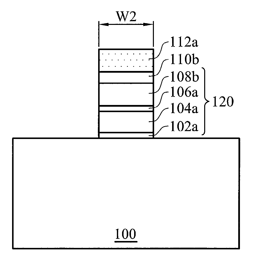
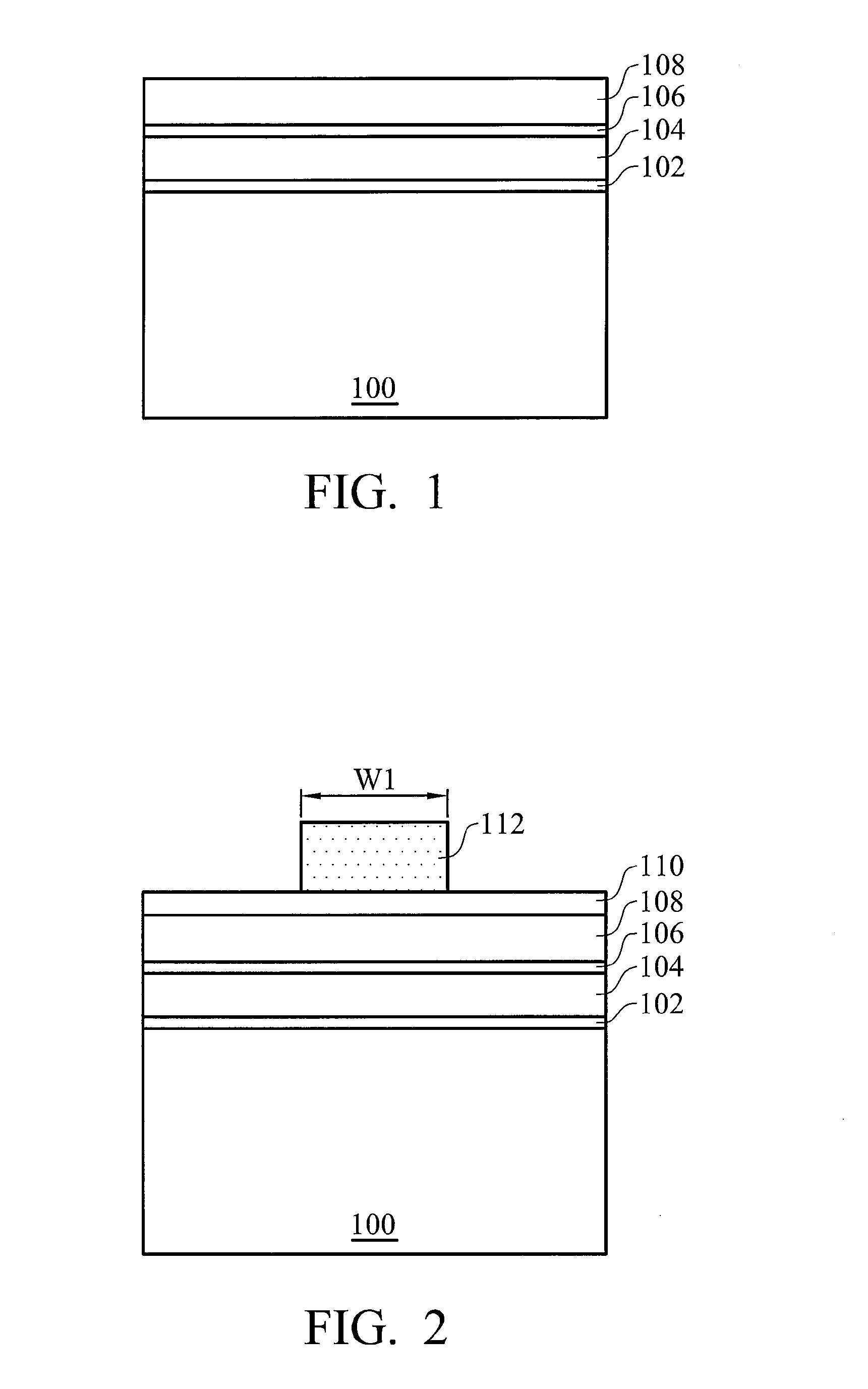
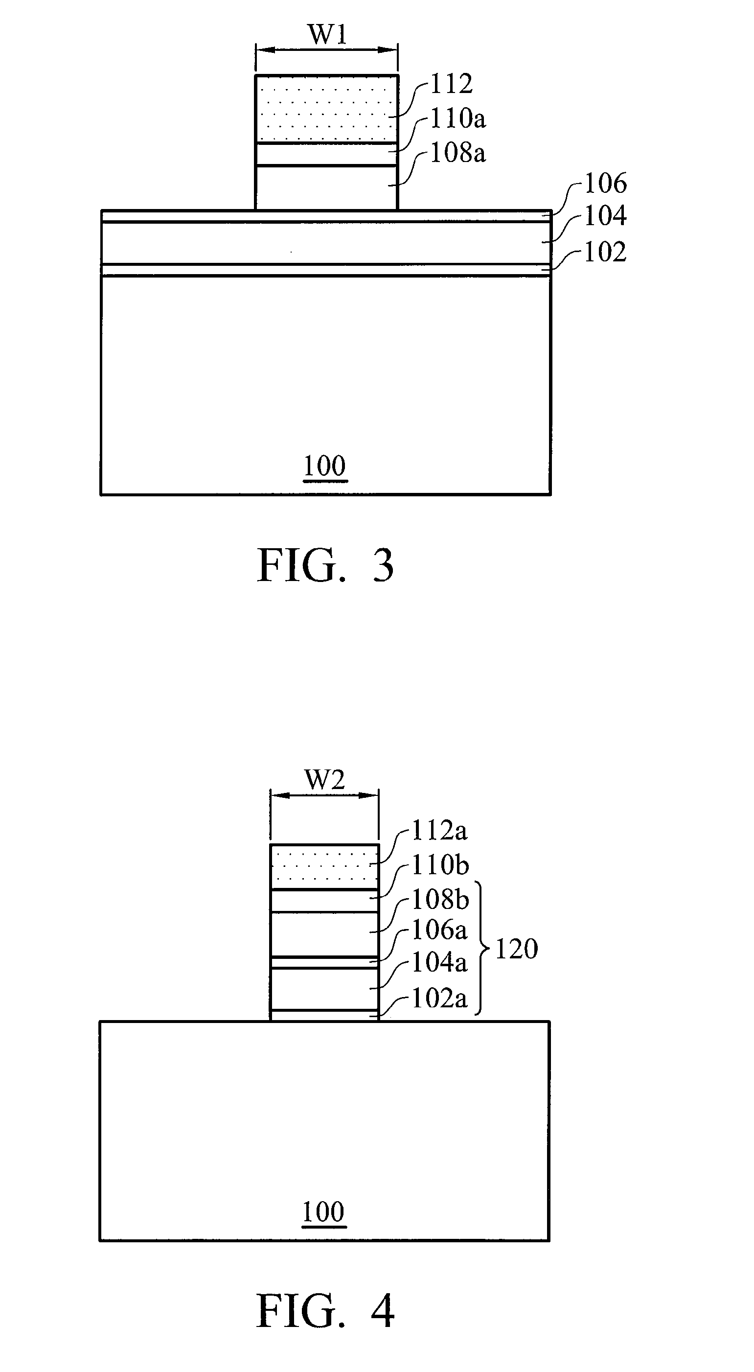
[0019]As shown in FIG. 1, a semiconductor substrate 100 such as a silicon substrate or a silicon / Germanium substrate is provided. A first oxide film 102 such as silicon oxide having a thickness of about 50 Å to 100 Å is optionally formed on the semiconductor substrate 100 by thermal oxidation. The first oxide film 102 may enhance adhesion between the semiconductor substrate 100 and first masking layer 104 formed in the following step.

[0020]A first masking layer 104 such as silicon nitride (Si3N4) is formed on the first oxide film 102 by chemical vapor deposition such as plasma enhanced chemical vapor deposition (PECVD), low pressure chemical vapor deposition (LPCVD) us...


PUM


Abstract

A fin field effect transistor and method of forming the same. The fin field effect transistor comprises a semiconductor substrate having a fin structure and between two trenches with top portions and bottom portions. The fin field effect transistor further comprises shallow trench isolations formed in the bottom portions of the trenches and a gate electrode over the fin structure and the shallow trench isolation, wherein the gate electrode is substantially perpendicular to the fin structure. The fin field effect transistor further comprises a gate dielectric layer along sidewalls of the fin structure and source/drain electrode formed in the fin structure.

Description

BACKGROUND OF THE INVENTION[0001]1. Field of the Invention[0002]The present invention relates generally to the field of semiconductor manufacturing and, more specifically, to a fin field effect transistor and method of forming the same.[0003]2. Description of the Related Art[0004]A fin field effect transistor (FinFET) such as a double gate MOSFET structure consists of a channel formed in a vertical silicon fin. FinFETs have found wide application as electronic devices for example, in digital processing applications. FinFETs, like other transistor devices, continue to be scaled to smaller and smaller dimensions in order to improve integrated circuit performance and cost. As the FinFET device is further miniaturized, device density will increase. It also becomes increasingly technically challenging to fabricate the FinFET features in the needed smaller dimensions.[0005]The needed width of the fin structure is beyond the resolution limit or capabilities using the lithographic technique...

Claims


Application Information

Patent Timeline
IPC IPC(8): H01L21/336H01L29/76
CPCH01L29/66795H01L29/7853H01L29/7851H01L29/0649
Inventor HSU, JU-WANGTING, CHIH-YUANZHONG, TANG-XUANSU, YI-NIENTSAI, JANG-SHIANG
Owner TAIWAN SEMICON MFG CO LTD
Why Eureka
Try Eureka