

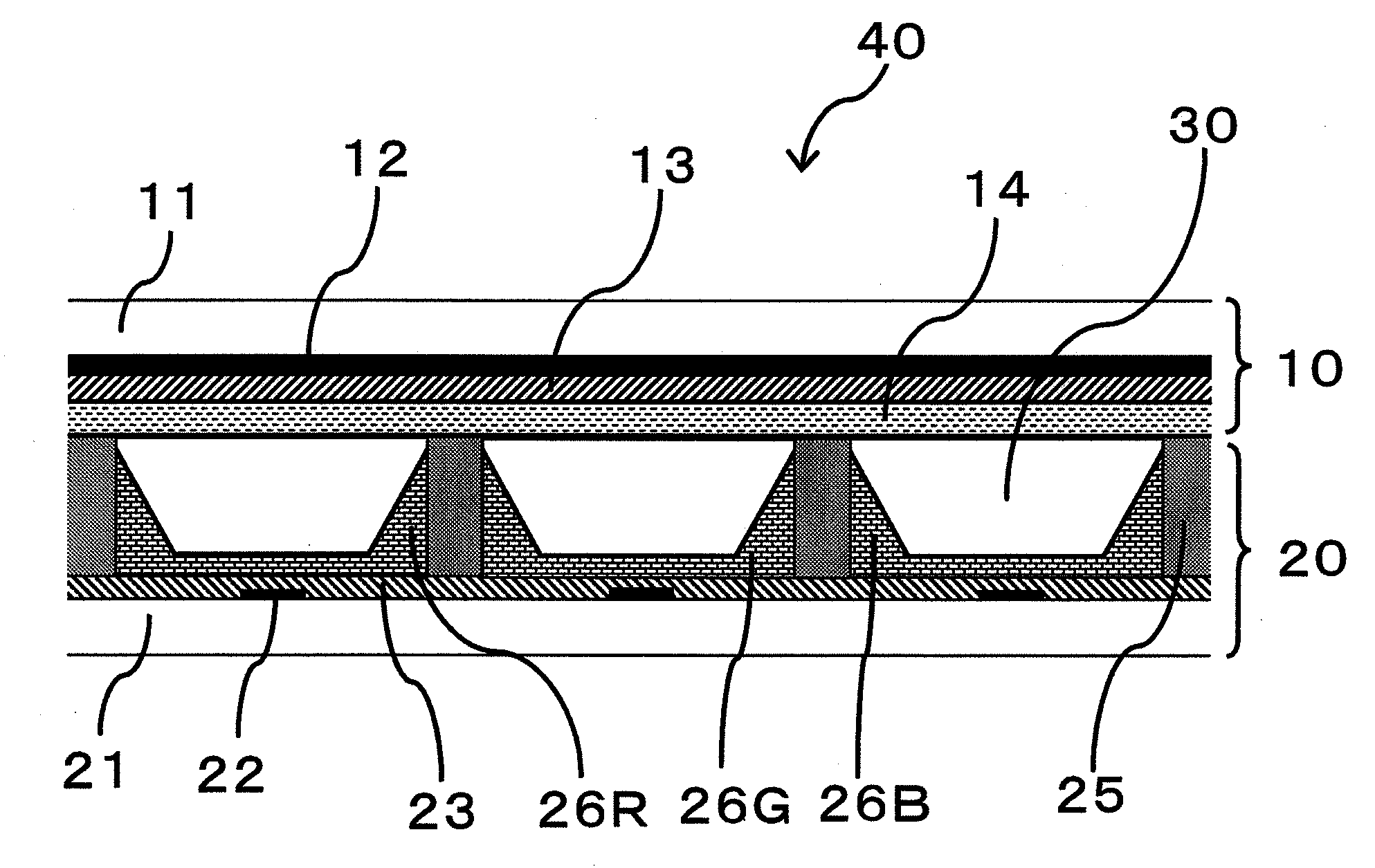
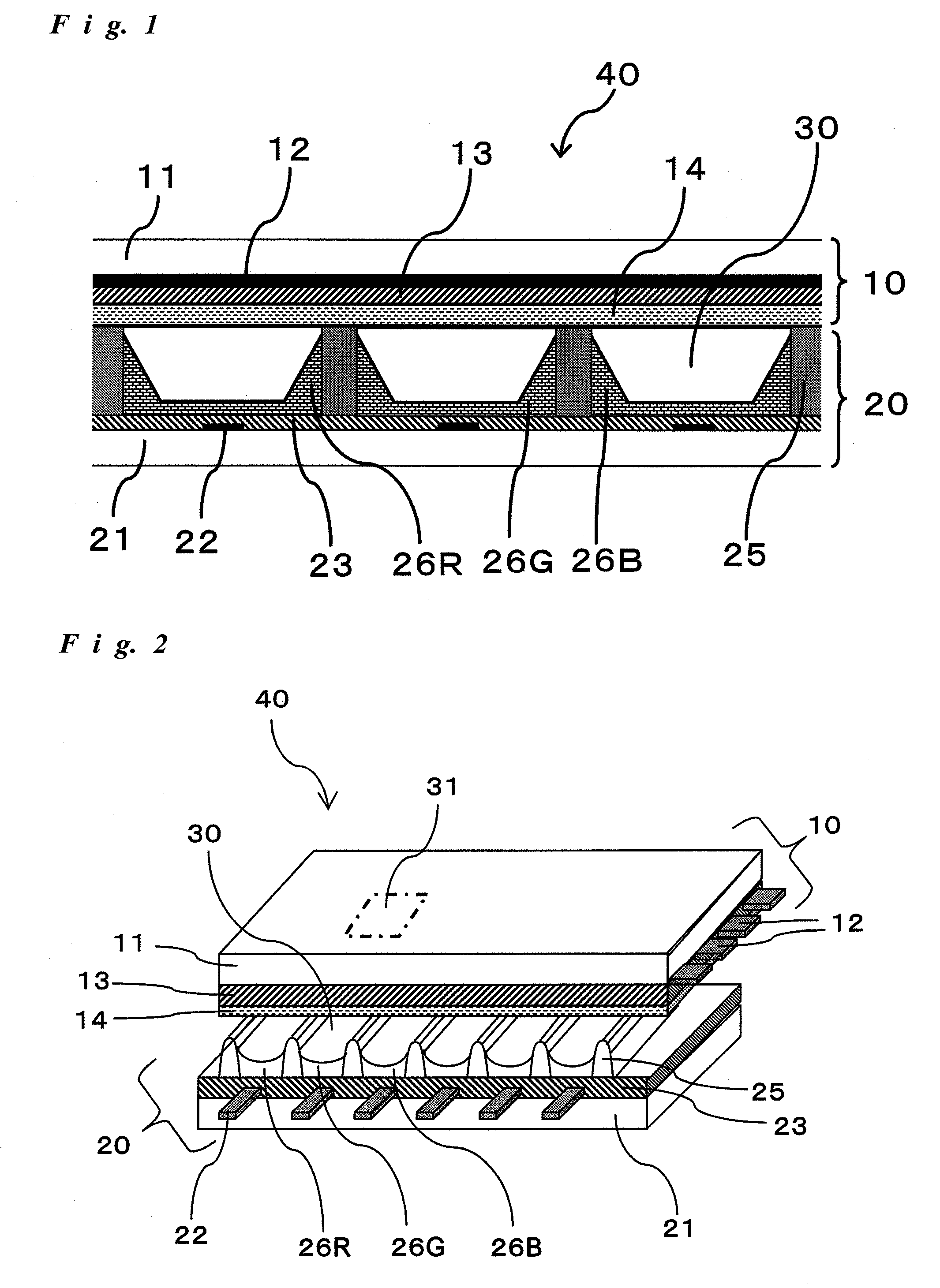
Plasma display panel and method for producing the same
a technology of plasma display panel and display panel, which is applied in the manufacture of electrode systems, electric discharge tube/lamps, discharge tube luminescnet screens, etc., can solve the problems of low panel brightness, achieve a higher definition of plasma display panels, reduce the effect of dielectric layer yellowing, and resist the phenomenon of dielectric breakdown
- Summary
- Abstract
- Description
- Claims
- Application Information
AI Technical Summary
Benefits of technology
Problems solved by technology
Method used
Image

Examples
examples
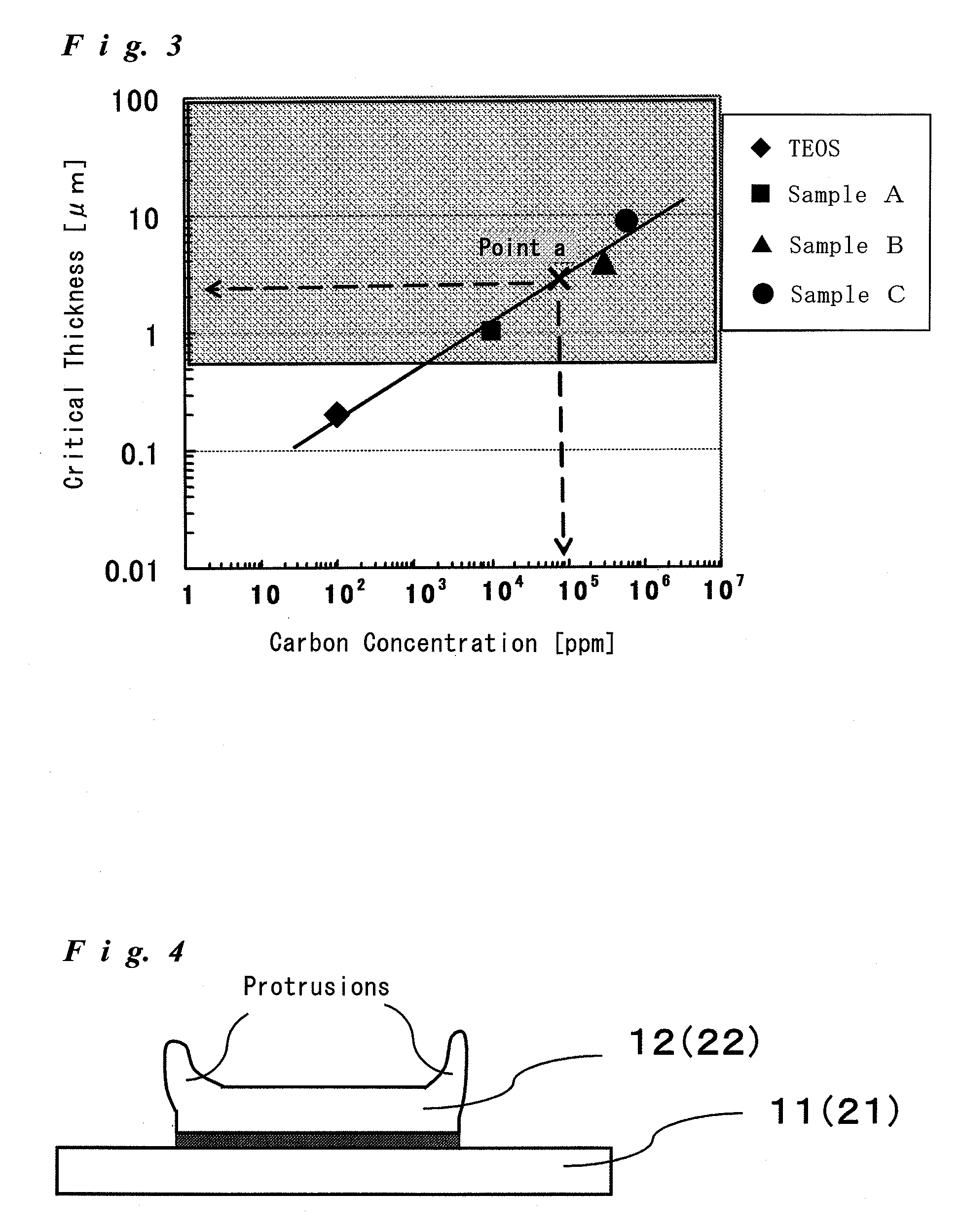
[0131]Test to Obtain Correlation between Carbon Concentration and Dielectric Layer Thickness
[0132]The test was conducted to obtain the correlation between “carbon concentration (ppm) of dielectric layer” and “critical thickness (μm) of dielectric layer”. To this end, firstly, a dielectric material paste was applied on a glass substrate (L×W×H: 12.5 cm×12.5 cm×1.8 cm, Nippon Electric Glass Co., Ltd.) to form a thin film consisting of the dielectric material. Subsequently, the thin film was dried at 150° C. for 10 minutes, and then was calcined at 500° C. for 1 hour. As a result, a dielectric layer was obtained on the glass substrate.
[0133]Specifically, the dielectric layers were formed from the following four kinds of the dielectric material pastes while changing the thickness of the thin film formed on the glass substrate, so as to determine the problem-free thickness above which there is occurred no peeling and no cracking in the dielectric layer (namely, so as to determine the cri...
PUM
 Abstract
Description
Claims
Application Information