Gas Discharge Display Panel

a display panel and gas discharge technology, applied in the manufacture of electric discharge tubes/lamps, electrode systems, cold cathode manufacturing, etc., can solve the problems of discharge delay, characteristic change of protective layer, and easy “discharge delay” of conventional protective layers, so as to reduce the gas absorption of protective layers, widen the driving margin, and improve reliability

Inactive Publication Date: 2008-11-13
PANASONIC CORP
View PDF6 Cites 10 Cited by
  • Summary
  • Abstract
  • Description
  • Claims
  • Application Information

AI Technical Summary

Benefits of technology

[0037]In the PDP of the present invention, the protective layer includes a first protective film and a second protective film, the second protective film is formed on at least part of a surface of the first protective film, and the first protective film has a larger content of the stated impurities, than the second protective film. According to the stated structure, during processes performed in the atmospheric air, gas absorption by the protective layer is reduced, and the discharge starting voltage is reduced to widen the driving margin, thereby enabling the PDP to exhibit more reliability with enhanced display quality free from black noise.
[0038]In addition, according to the manufacturing method of the PDP of the present invention, the protective layer is formed by forming a first protective layer on the surface of the dielectric layer, and then by forming a second protective film on at least part of a surface of the first protective film under the condition where an atmospheric air is blocked, the first protective film having a larger impurity content than the second protective layer. According to this manufacturing method of the PDP, the manufacturing cost lowers by reduction of the exhaustion time in the sealing exhaustion process, and the driving circuit cost is reduced.

Problems solved by technology

The first problem is that conventional protective layers are susceptible to “discharge delay”.
If the discharge delay is large, the possibility of preventing address discharge from occurring even at the end of the address pulse application becomes high, with which writing defect is likely caused.
The problem of discharge delay is a problem to be solved for improving image display performance of PDPs.
The second problem is a characteristic change of the protective layer.
In a process performed in the air from among the PDP manufacturing processes, a protective layer made of MgO tends to be contaminated by absorption of oil impurity, CO2, and H2O.
When the absorption gas is absorbed by the surface of the MgO, the characteristic of the protective layer changes, thereby decreasing the secondary electron emission efficiency.
This would lead to a problem of display defect called “black noise” which specifically is a phenomenon in which accurate display of intended cells is impaired.

Method used


Image

  • Gas Discharge Display Panel
  • Gas Discharge Display Panel
  • Gas Discharge Display Panel

Examples


first embodiment

[0040]1-1. Structure of PDP

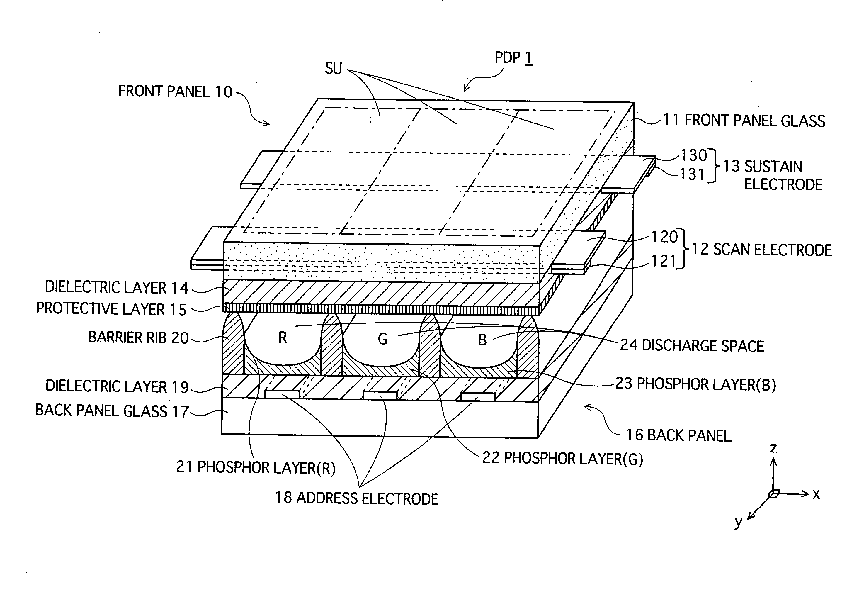
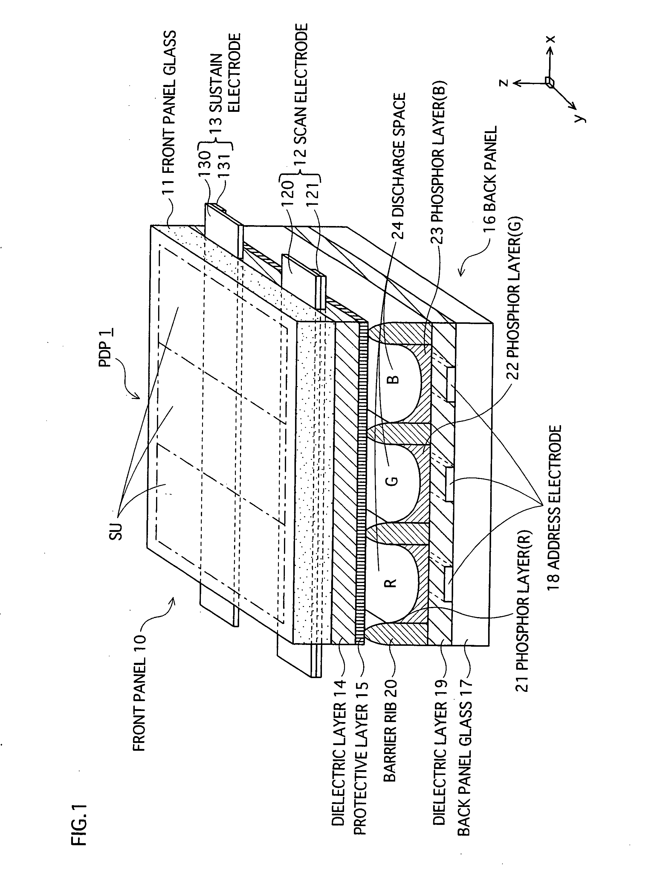
[0041]FIG. 1 is a partial perspective view showing a main structure of an AC-type PDP 1, according to the first embodiment of the present invention. In the drawing, the z-direction corresponds to a thickness direction of the PDP 1, and the xy plane corresponds to a plane parallel to the surface of the panels of the PDP 1. Here, the PDP 1 has an NTSC specification of 42 inches for example. However needless to say, the present invention is also applicable to other specifications, including XGA, and SXGA. The present invention is also applicable to other sizes.

[0042]As FIG. 1 shows, the PDP 1 is mainly structured by a front panel 10 and a back panel 16 whose main surfaces are opposed to each other.

[0043]On one main surface of the front panel glass 11 that is a substrate of the front panel 10, a plurality of pairs of display electrodes 12 and 13 (scan electrode 12 and sustain electrode 13) are provided. Each display electrode 12, 13 is formed by stacking bus l...

embodiment examples

and Confirmation Test for Advantageous Effect Thereof

[0071]FIG. 3 illustrates a graph for showing compositions of a protective layer and a relative size of a variation in discharge delay time (discharge variability). In this drawing, data relating to protective layers having the following structures is presented with the discharge variability of a conventional protective layer solely made of MgO being assumed as 100%.[0072]Si added protective layer (comparison example 2): 100 mass ppm of Si is added to MgO.[0073]Si+H added protective layer (first embodiment): 100 mass ppm of Si, and 1000 mass ppm of H are added to MgO.[0074]H added protective layer (second embodiment): 1000 mass ppm of H is added to MgO.

[0075]From the data in FIG. 3, the protective layer, (comparison example 2) with only Si addition in comparatively a small amount to MgO is considered as undesirable because the value of discharge variability is 114% which indicates performance deterioration even compared to the conv...

modification example 1

[0175]In the present modification example 1, first, a film mainly composed of MgO and additionally containing Si or Ge is formed using the method described in the first embodiment.

[0176]Then, means for generating H ion is used as a method of doping the H atoms to the film, thereby irradiating H ion on the surface of the formed film.

[0177]Here, the setting conditions are as follows for example: using a heater, the substrate is heated to the temperature of 100-300 degrees Celsius within the doping chamber of H atoms, and the chamber is evacuated until the vacuum level reaches 1×10⁻⁴-7×10⁻⁴ Pa.

[0178]After this, H ions are irradiated onto the protective layer 15 having been formed on the substrate using an ion gun linked to the H container, thereby doping H atoms of the protective layer 15. The amount of flowing for H is set in the range of 1×10⁻⁵-3×10⁻⁵ m3 / min.


PUM

PropertyMeasurementUnit
thicknessaaaaaaaaaa
thicknessaaaaaaaaaa
widthaaaaaaaaaa

Abstract

Provided is a gas discharge display panel that exhibits a favorable display performance by maintaining a wall charge retaining power, controlling discharge delay within a range adequate for optimal image display, and reducing the discharge starting voltage at comparatively low cost. Also provided is a PDP that exhibits more reliability with enhanced display quality by further improving the secondary electron emission factor γ compared to conventional cases and lowering the discharge starting voltage to widen the driving margin. Further provided is a manufacturing method of a gas discharge display panel, by which the manufacturing cost lowers by reduction of the exhaustion time in the sealing exhaustion process, and by which the driving circuit cost is reduced. In a gas discharge display panel of the present invention, a protective layer (15) has a first protective film (151) and a second protective film (152), the second protective film (152) is formed on at least part of a surface of the first protective film (151), and the first protective film (151) has a larger impurity content than the second protective film (152).

Description

TECHNICAL FIELD[0001]The present invention relates to a gas discharge display panel such as a plasma display panel. The present invention particularly relates to a technology for improving a protective layer.BACKGROUND ART[0002]Gas discharge display panels, represented by a plasma display panel (hereinafter simply “PDP”), a redisplay apparatuses that display images by light emission performed by exciting phosphors by means of ultraviolet light generated by gas discharge. According to the discharge forming method, PDPs are divided into two types of alternating current (AC) type and direct current (DC) type, where the AC type is most common because of superiority over the DC type in terms of brightness, light emission efficiency, and lifetime.[0003]As is disclosed in Patent reference 1 for example, an AC-type PDP has the following structure. Two thin glass panels respectively provided with a plurality of electrodes (either display electrodes or address electrodes) and a dielectric lay...

Claims


Application Information

Patent Timeline
Patent Type & Authority Applications(United States)
IPC IPC(8): H01J17/49H01J9/02
CPCH01J11/12H01J11/40C23C14/081H01J11/38
Inventor YAMAMOTO, SHINICHINISHITANI, MIKIHIKOTERAUCHI, MASAHARUHASHIMOTO, JUNKITAGAWA, MASATOSHI
Owner PANASONIC CORP
Why Eureka
Try Eureka