Semiconductor memory device and method for correcting memory cell data

a memory cell and memory technology, applied in the field of semiconductor memory devices and a method for correcting data stored in memory cells, can solve the problems of wasting power, affecting the operation of memory cells, etc., and achieves the effect of low power consumption and unnecessary stresses

Active Publication Date: 2005-11-22
III HLDG 12 LLC
View PDF2 Cites 23 Cited by
  • Summary
  • Abstract
  • Description
  • Claims
  • Application Information

AI Technical Summary

Benefits of technology

[0019]That is, since it is sufficient to correct the memory cell only when the physical quantity is out of the...

Problems solved by technology

Conventionally, in flash memories, which is known as electrically programmable and erasable nonvolatile memories, problems can occur in which a charge state, which is one factor representing a physical quantity corresponding to data to be stored into individual memory cells, is varied by stresses.
This leads to potential problems of causing, for example, delays in access time and read errors.
This gives rise to problems such as that it takes a time for the processing, the shift of threshold due to variations in the charge amount which is one factor representing the physical quantity cannot be sensed in an early stage, and in addition, reduction in power consumption cannot be implemented.
In addition, each time a threshold shift is sensed, stresses are imposed on the memory cell, thereby increasing the pr...

Method used


Image

  • Semiconductor memory device and method for correcting memory cell data
  • Semiconductor memory device and method for correcting memory cell data
  • Semiconductor memory device and method for correcting memory cell data

Examples


Embodiment Construction

[0030]An embodiment of a semiconductor memory device of the invention will be described hereinbelow with reference to the accompanying drawings.

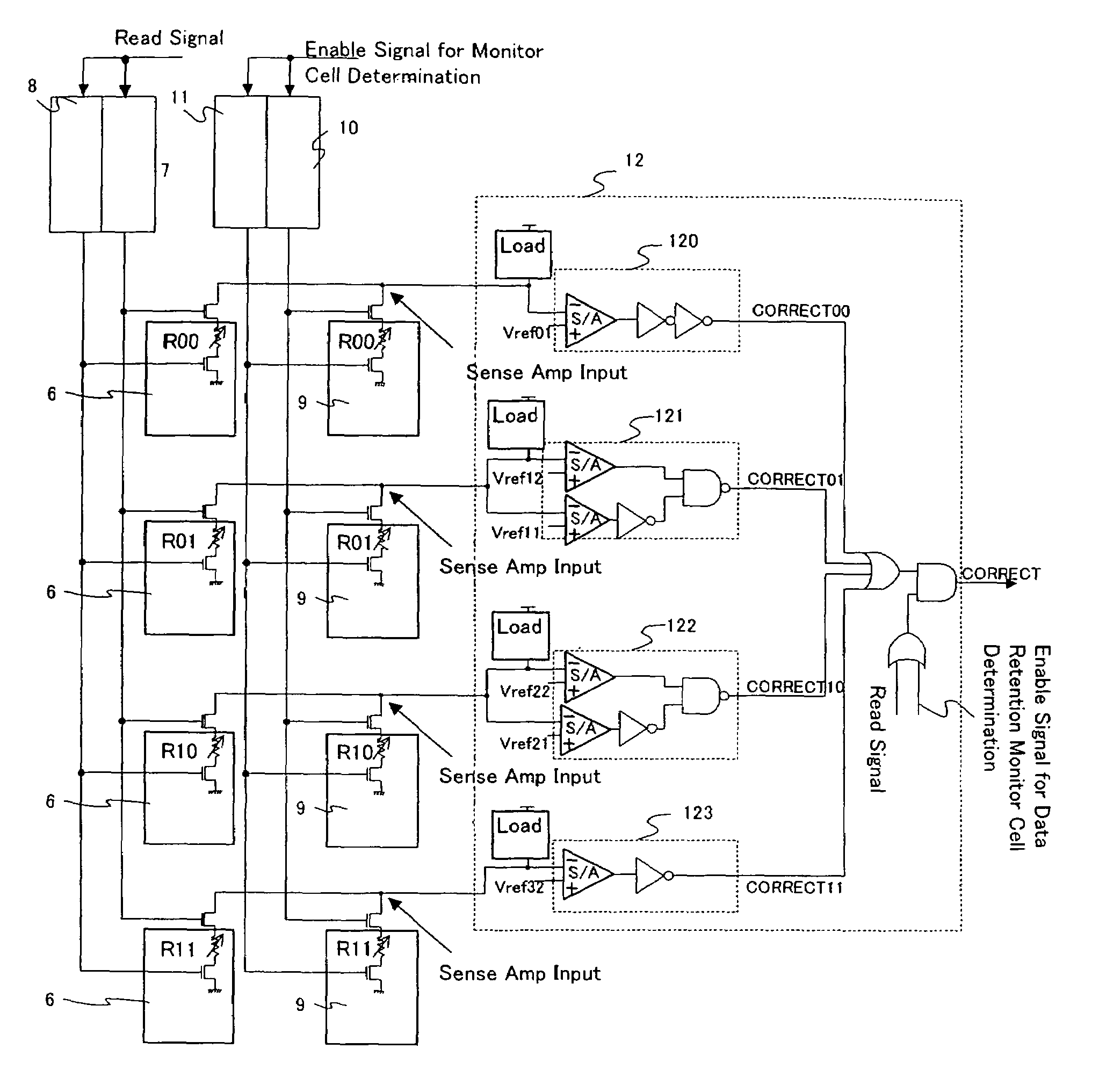
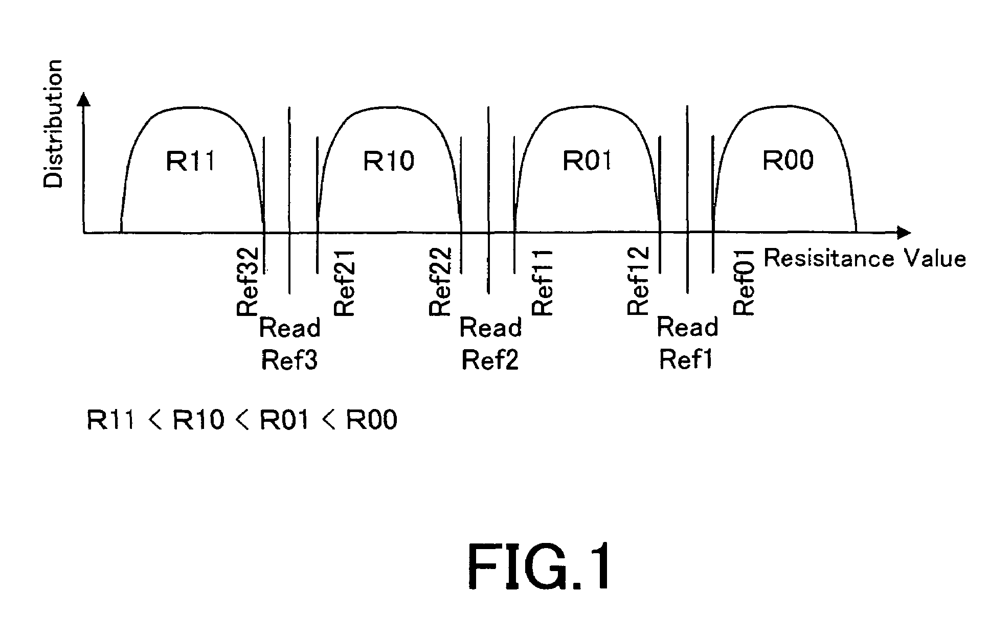
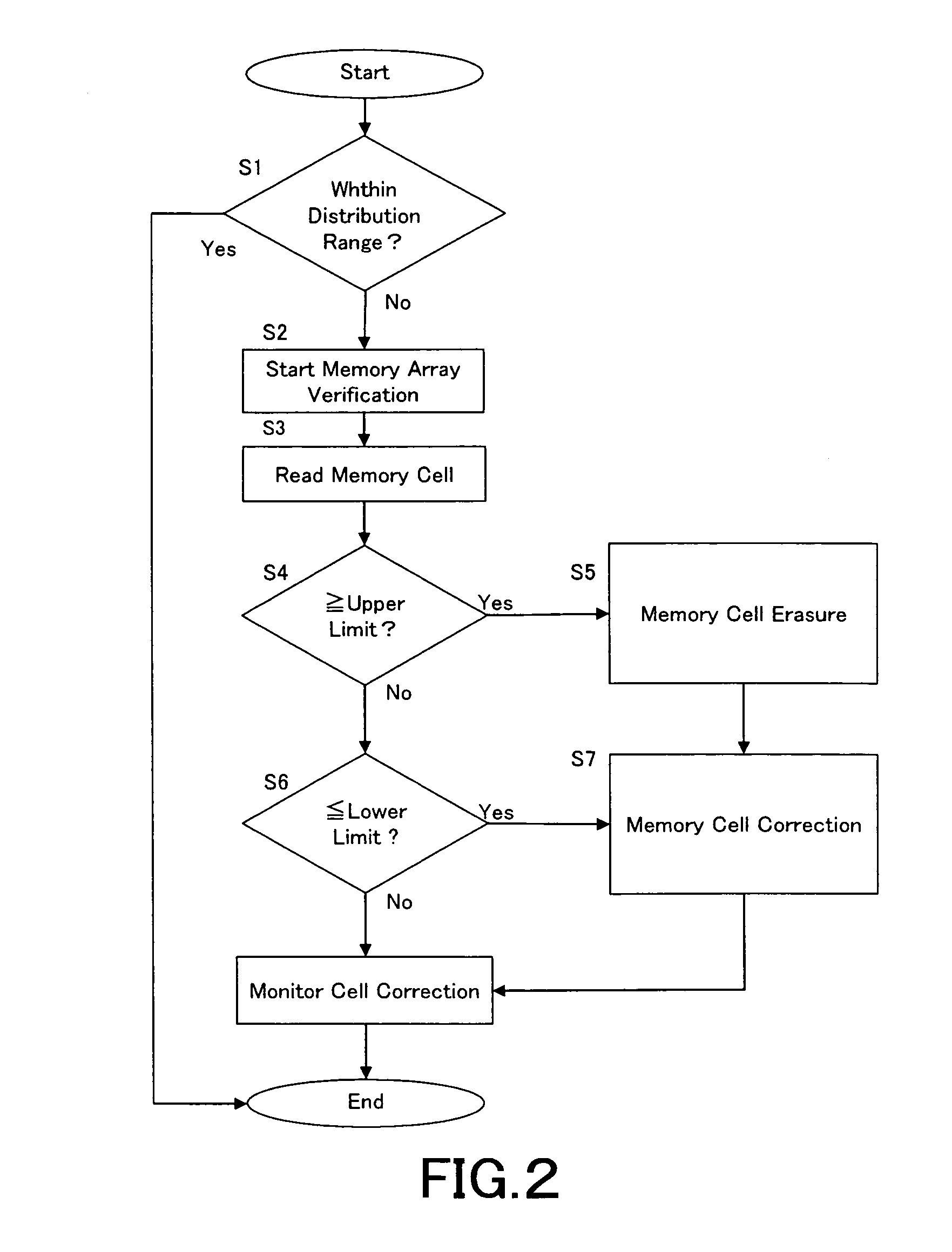
[0031]Referring to FIG. 3, the flash memory is configured to include, for example, a memory array 1, a reference array 2, a row decoder 4, a column decoder 5, a voltage switch 14, a command interface 15, and a control engine 16. The memory array 1 has a plurality of memory cells arranged in a matrix, each of which is capable of storing N-level data (N represents a natural number of 2 or greater) and being reprogrammed. The reference array 2 contains stored reference data input to one end of a sense circuit 3. The row decoder 4 outputs word line selection signals that individually select word lines, and the column decoder 5 outputs bit-line selection signals that individually select bit lines. The voltage switch 14 has a function of switching among voltages for supply to individual circuits corresponding to individual modes such as program, e...


PUM


Abstract

A semiconductor memory device comprises a plurality of memory cells, each of which is capable of storing N-level data and being reprogrammed; and a plurality of monitor cells that separately store individual data values of the N-level data by using the same scheme as that used for the memory cells. Sensing means senses whether a physical quantity of the monitor cell which corresponds to the data value stored in the monitor cell is within a preset range; verification means verifies whether the physical quantity of the memory cell which corresponds to the data value stored in the memory cell is within the preset range when the sensing means has sensed that the physical quantity of the monitor cell is out of the preset range; correction means corrects the physical quantity. Consequently, a physical quantity variation can be efficiently detected without overstressing memory cells, and correction can be implemented for not only a downward variation due to charge loss and/or the like but also a variation in an upward physical quantity variation due to charge gain and/or the like in a specified range.

Description

BACKGROUND OF THE INVENTION[0001]1. Field of the Invention[0002]The present invention relates to a semiconductor memory device and a method for correcting data stored in memory cells.[0003]2. Description of the Related Art[0004]Conventionally, in flash memories, which is known as electrically programmable and erasable nonvolatile memories, problems can occur in which a charge state, which is one factor representing a physical quantity corresponding to data to be stored into individual memory cells, is varied by stresses. The stresses can occur because of, for example, electric current / voltage during time transition and / or in the events of a data read and the like, whereby threshold distributions of the individual memory cells deviates from a specified range. This leads to potential problems of causing, for example, delays in access time and read errors. To overcome these problems, U.S. Pat. No. 5,835,413 proposes a technique for performing data correction for a memory cell with a th...

Claims


Application Information

Patent Timeline
IPC IPC(8): G11C16/06G11C13/00G11C11/56G11C16/34G11C11/15G11C16/10G11C16/02G11C29/00G11C29/42
CPCG11C11/5678G11C11/5685G11C13/0007G11C13/0064G11C13/0069G11C16/3431G11C13/0033G11C13/0004G11C2213/31G11C29/00G11C16/10
Inventor HAMAGUCHI, KOJI
Owner III HLDG 12 LLC
Why Eureka
Try Eureka