Method of manufacturing a semiconductor integrated circuit device

Active Publication Date: 2008-11-20
RENESAS ELECTRONICS CORP
View PDF6 Cites 15 Cited by
  • Summary
  • Abstract
  • Description
  • Claims
  • Application Information

AI Technical Summary

Benefits of technology

[0026]In the chip with which a plurality of MISFET from which threshold value voltage differs is intermingled, leaka

Problems solved by technology

However, in mobile communications apparatus by which the standby current value in room temperature atmosphere constitutes important specification, for example, such as a cellular phone, the pro

Method used


Image

  • Method of manufacturing a semiconductor integrated circuit device
  • Method of manufacturing a semiconductor integrated circuit device
  • Method of manufacturing a semiconductor integrated circuit device

Examples


embodiment 1

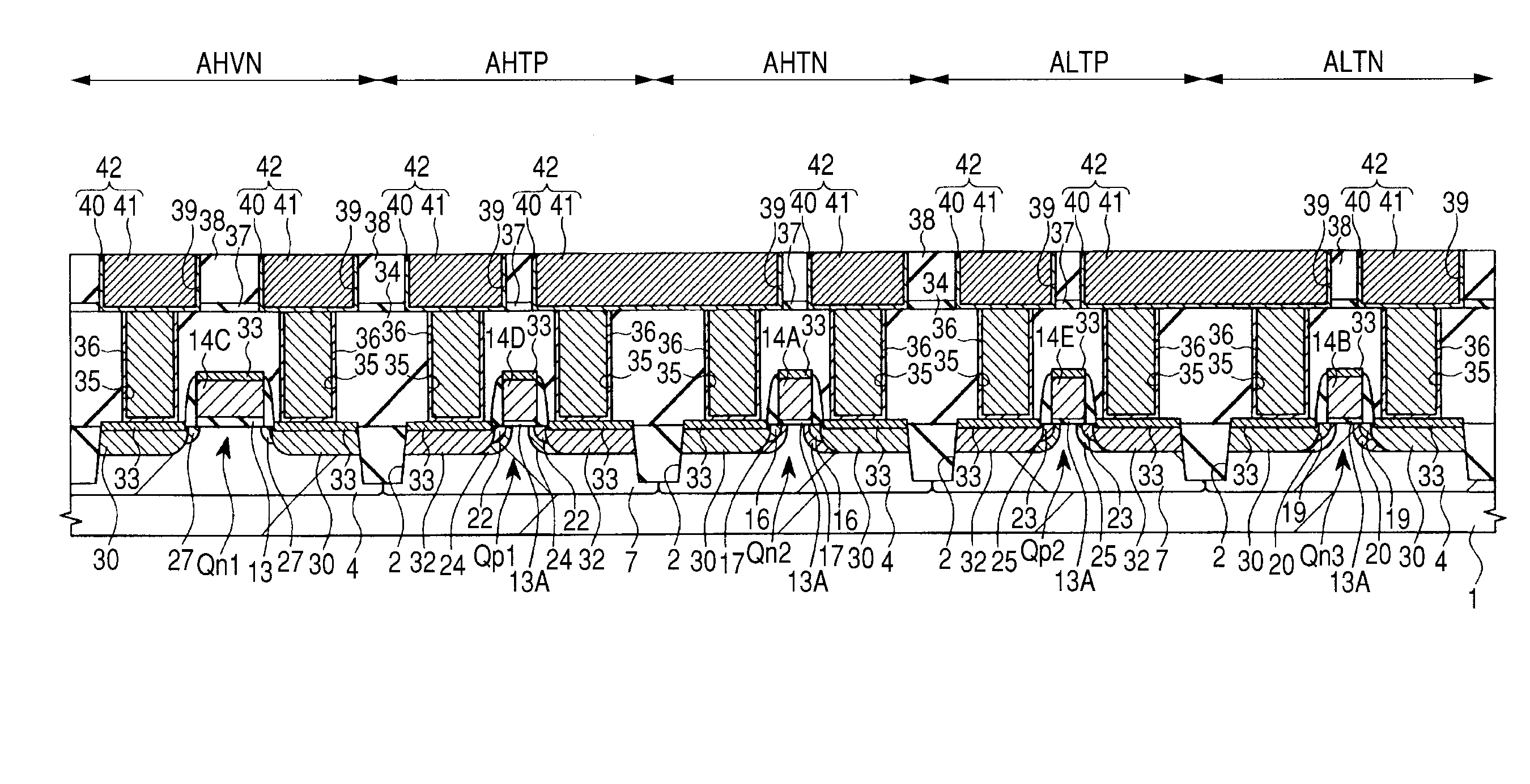
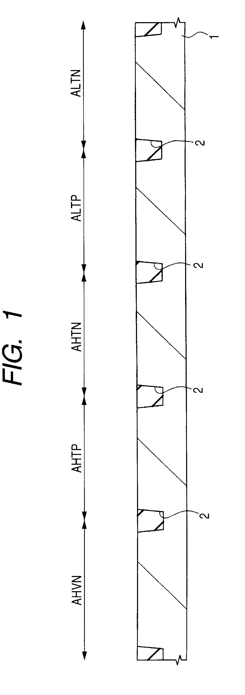
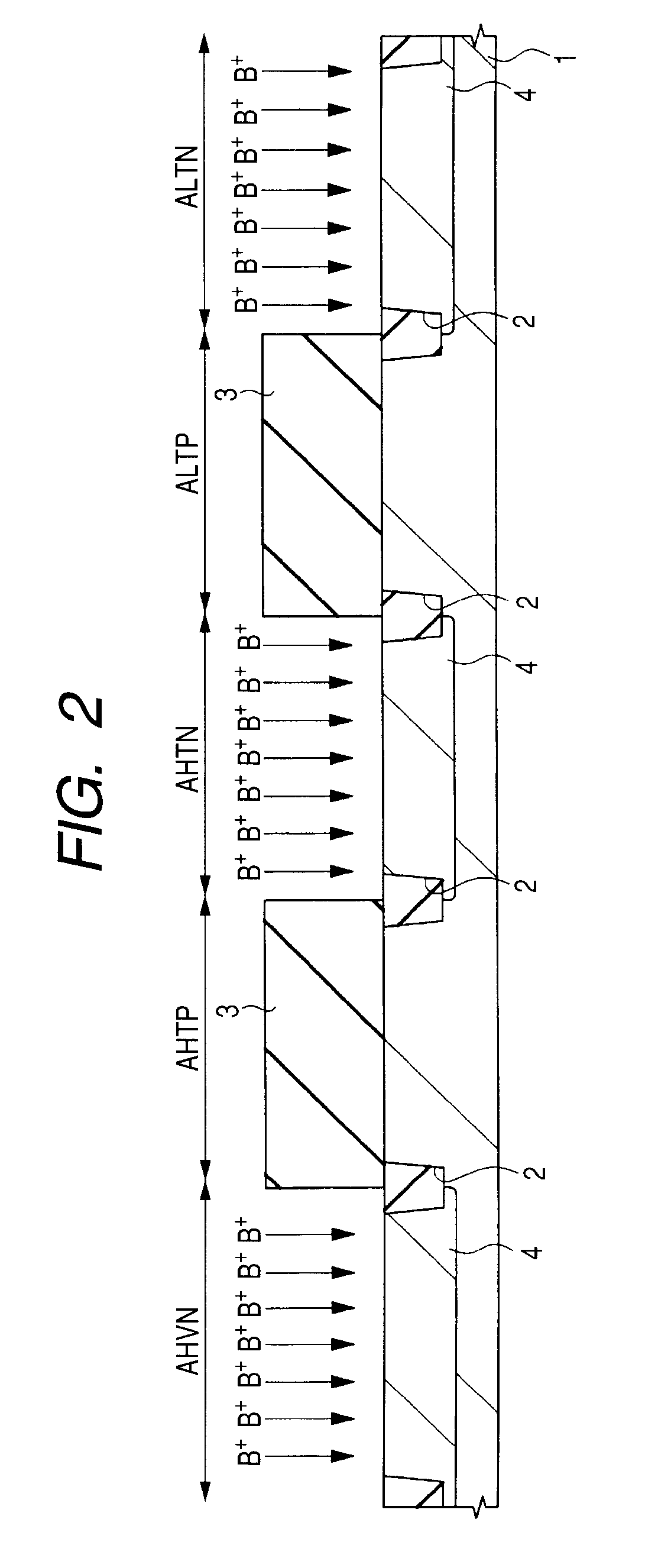
[0093]The semiconductor integrated circuit device of Embodiment 1 includes the CMOS logic LSI mounted, for example in mobile communications apparatus, such as a cellular phone. The manufacturing process of the semiconductor integrated circuit device of such Embodiment 1 is explained to process order using FIG. 1-FIG. 22.

[0094]FIG. 1-FIG. 22 show the principal part section of the semiconductor substrate (it is merely hereafter described as a substrate) in the manufacturing process of the semiconductor integrated circuit device of Embodiment 1 to process order, and show the section of the same part of the substrate, respectively. The logical circuit, the input and output circuit, etc. are formed in CMOS logic LSI. MISFET with relatively high threshold value voltage and MISFET with relatively low threshold value voltage are included in MISFET which forms the logical circuit. Into the portion which determines the working speed of a circuit among MISFET which forms a logical circuit, MIS...

embodiment 2

[0139]In Embodiment 2, in addition to MISFET with relatively high threshold value voltage (n channel type MISFET Qn2 (refer to FIG. 18) and p channel type MISFET Qp1 (refer to FIG. 19)), MISFET with relatively low threshold value voltage (n channel type MISFET Qn3 (refer to FIG. 18) and p channel type MISFET Qp2 (refer to FIG. 19)), and MISFET (n channel type MISFET Qn1 (refer to FIG. 18)) with a relatively large breakdown voltage explained in the Embodiment 1, MISFET which has the threshold value voltage between MISFET with relatively high threshold value voltage and MISFET with relatively low threshold value voltage is also formed in the same substrate 1.

[0140]FIG. 23-FIG. 42 show the principal part section of substrate 1 in the manufacturing process of the semiconductor integrated circuit device of Embodiment 2 to process order, and show the section of the same part of substrate 1, respectively. In FIG. 23-FIG. 42, in addition to region AHTN, AHTP, ALTN, ALTP, and AHVN explained ...

embodiment 3

[0160]In Embodiment 3, in addition to MISFET with relatively high threshold value voltage (n channel type MISFET Qn2 (refer to FIG. 18) and p channel type MISFET Qp1 (refer to FIG. 19)), MISFET with relatively low threshold value voltage (n channel type MISFET Qn3 (refer to FIG. 18) and p channel type MISFET Qp2 (refer to FIG. 19)), and MISFET (n channel type MISFET Qn1 (refer to FIG. 18)) with a relatively large breakdown voltage explained by the Embodiment 1, MISFET which forms the memory cell of SRAM (Static Random Access Memory) is also formed in the same substrate 1. As the Embodiment 1 also described, the MISFET with relatively high threshold value voltage and MISFET with relatively low threshold value voltage form the logical circuit mounted in mobile communications apparatus. The semiconductor integrated circuit device in which this logical circuit was formed is asked for low power consumption property. MISFET which forms the memory cell of SRAM of Embodiment 3 is asked for ...


PUM


Abstract

In the chip with which a plurality of MISFET from which threshold value voltage differs is intermingled, leakage current, such as GIDL current and BTBT current, is suppressed, inhibiting the short channel effect of MISFET. The concentration of the impurity for threshold value voltage adjustment implanted to the region in which n channel type MISFET with relatively low threshold value voltage is formed is made lower than the concentration of the impurity for threshold value voltage adjustment implanted to the region in which n channel type MISFET with relatively high threshold value voltage is formed. Implantation amount of the impurity at the time of forming n type semiconductor region 19 and punch-through stopper layer 20 in region ALTN is made larger than the implantation amount of the impurity at the time of forming n type semiconductor region 16 and punch-through stopper layer 17 in region AHTN, respectively.

Description

CROSS-REFERENCE TO RELATED APPLICATION[0001]The present application claims priority from Japanese patent application No. 2007-129547 filed on May 15, 2007, the content of which is hereby incorporated by reference into this application.FIELD OF THE INVENTION[0002]The present invention relates to the manufacturing technology of a semiconductor integrated circuit device, and particularly relates to an effective technology in the application to manufacture of the semiconductor integrated circuit device which has the semiconductor chip with which a plurality of transistors from which threshold value voltage differs were formed.DESCRIPTION OF THE BACKGROUND ART[0003]In Japanese patent laid-open No. 2003-100902 (Patent Reference 1), a semiconductor device with which a plurality of same channel type MOS's from which the impurity concentration in an extension layer and the impurity concentration in a pocket layer differ, and a breakdown voltage differs were formed on the same chip, and its m...

Claims


Application Information

Patent Timeline
IPC IPC(8): H01L21/8234
CPCH01L21/823807H01L21/823814
Inventor MINAMI, MASATAKA
Owner RENESAS ELECTRONICS CORP
Why Eureka
Try Eureka