Thick Crystalline Silicon Film On Large Substrates for Solar Applications

a technology of thin crystalline silicon and solar energy, which is applied in the direction of crystal growth process, sustainable manufacturing/processing, final product manufacturing, etc., can solve the problems of high raw material cost, high cost of harvesting, and high cost of raw materials

Inactive Publication Date: 2008-12-04
SOLAR NOTION
View PDF13 Cites 37 Cited by
  • Summary
  • Abstract
  • Description
  • Claims
  • Application Information

AI Technical Summary

Benefits of technology

[0014]In one embodiment of the invention, an apparatus for converting sunlight to electricity comprises a sheet of soda lime glass having a softening point not exceeding 600° C. and

Problems solved by technology

Although solar energy is free, but the cost to harvest it is still very high compared to conventional coal, petroleum, natural gas and nuclear energy.
The reasons for such slow price reduction are mainly attributed to the high cost of raw materials and complicated processes.
The demand on solar panels created a silicon wafer shortage in recent years.
Due to the lack of differentiation, these improvements are too slow to satisfy the market demand.
Therefore, most of the solar panel companies have yet to turn a substantial profit.
However the cost of ownership for such systems is actually higher because: (1) Lower efficiency means higher installation cost, slower return on investment due to limited roof space; (2) Shorter lifetime and (3) unproven reliability.
Therefore, they are still immature technologies and cost benefit, efficiency, and reliability are not yet established.
It is highly questionable that they can improve

Method used


Image

  • Thick Crystalline Silicon Film On Large Substrates for Solar Applications
  • Thick Crystalline Silicon Film On Large Substrates for Solar Applications
  • Thick Crystalline Silicon Film On Large Substrates for Solar Applications

Examples


Embodiment Construction

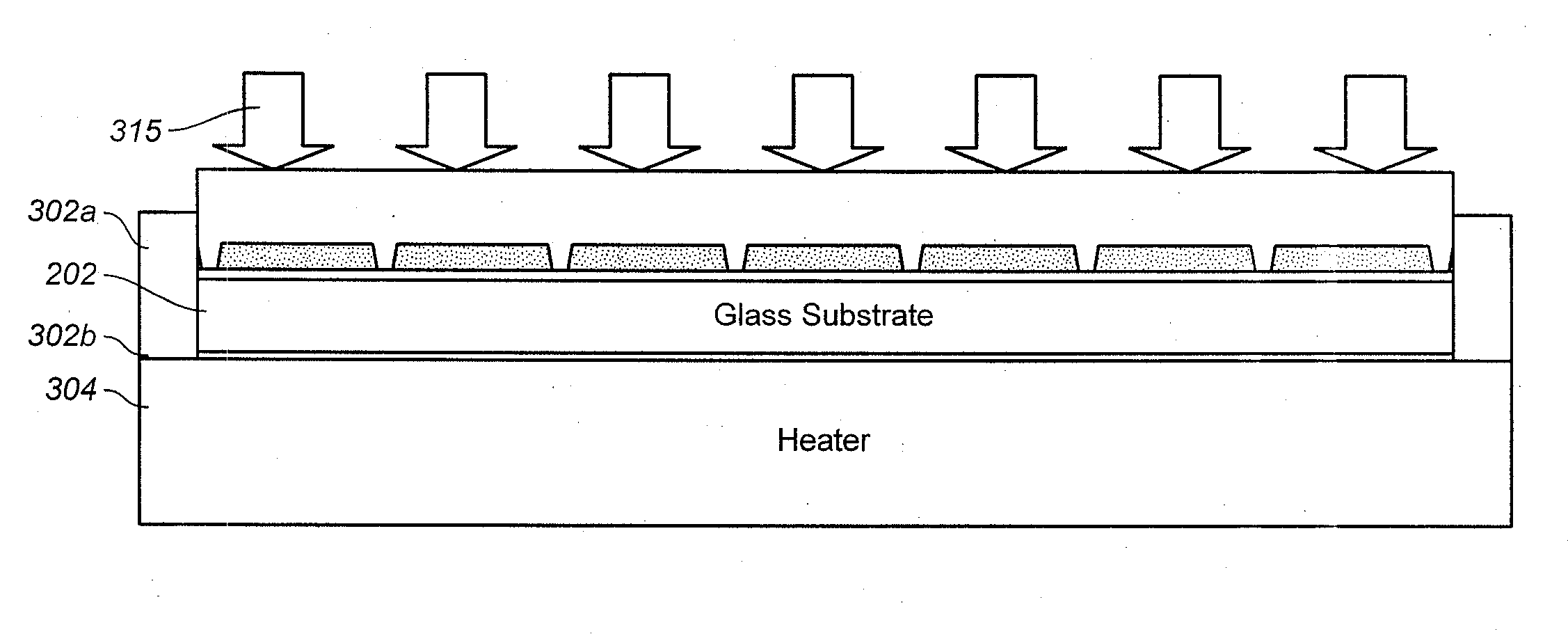
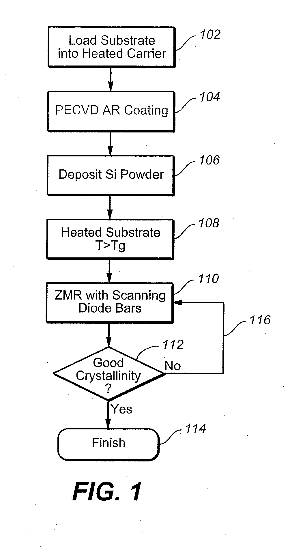
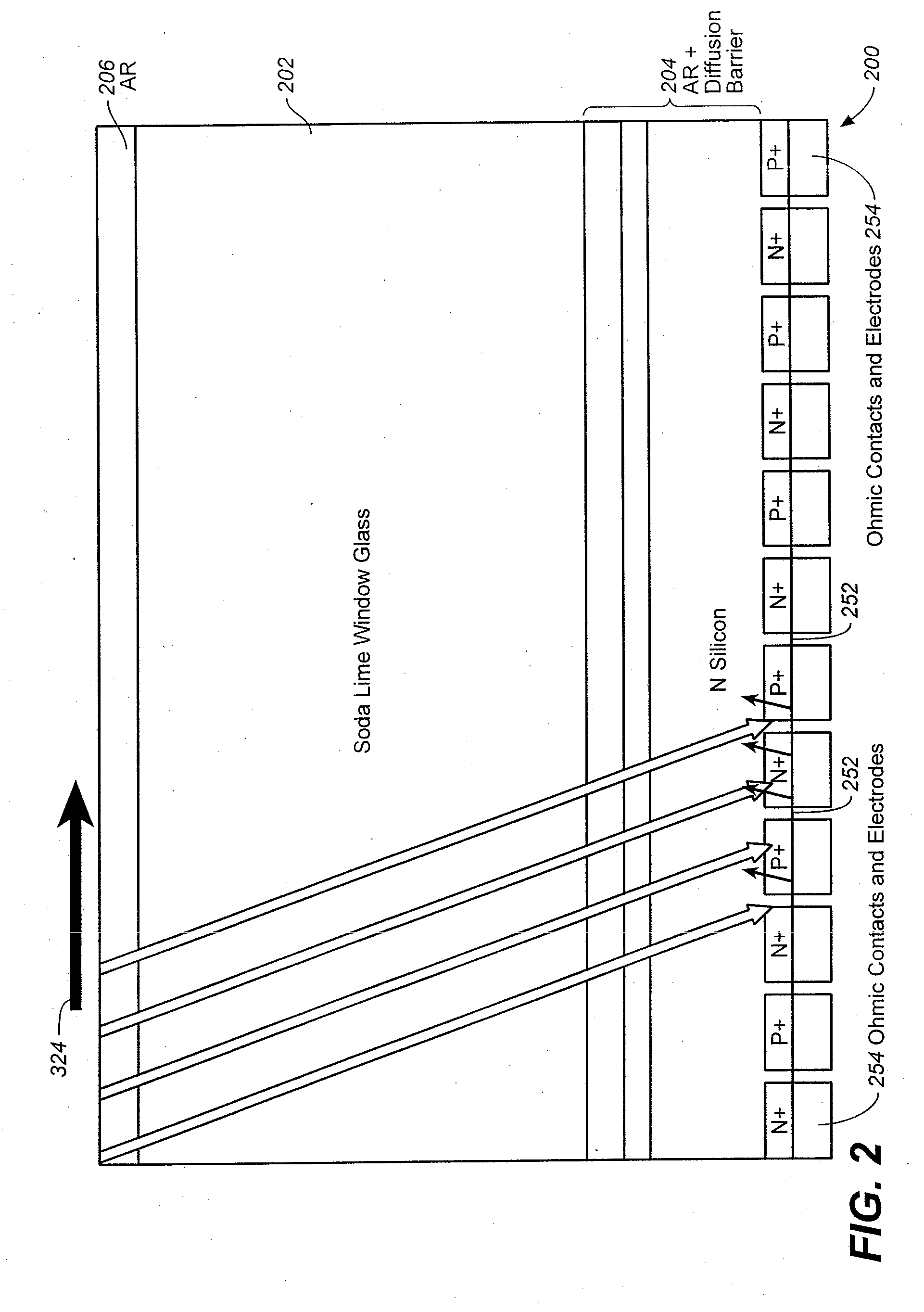
[0029]This invention discloses processes of making low cost, large scale, and high purity thick crystalline silicon film for solar cell. Thick silicon films (over 5 μm) are made on low temperature substrate. Soda lime glass (that is glass used in windows used in window of residential and commercial buildings) is of low cost and is widely available. A new process is used that combines substrate preparation, temperature control, use of silicon powder materials, and laser annealing to observe silicon thick films that is substantially crystalline. A schematic of the process flow is shown in FIG. 1.

[0030]A substrate is prepared and loaded onto a carrier (block 102). An anti-reflection (AR) coating is formed using the PECVD process (block 104). Silicon powder is then dispersed onto the AR coating (block 106). The carrier, substrate and the carrier are then heated to a temperature (e.g. 600° C.) greater than the softening point of the material of the substrate causing the substrate to soft...


PUM


Abstract

An apparatus for converting sunlight to electricity comprises a sheet of soda lime glass having a softening point not exceeding 600° C. and a layer of crystalline silicon over said sheet of soda lime glass. The layer has a thickness not less than about 5 microns and grains with grain size not less than about 100 microns. A method for making a device for converting sunlight to electricity comprises forming a film on a soda lime glass substrate, dispersing silicon powder onto the film and pressing a surface onto the silicon powder to form a layer of silicon powder on said film. The substrate and film are heated from below to a temperature so that the soda lime glass substrate softens. While the substrate is in a softened state, the silicon powder layer is heated by scanning a line focus laser beam or an elongated heater strip over a spatial sequence of adjacent elongated zones of the silicon powder consecutively so that the silicon powder in each of the zones melts and recrystallizes consecutively to form a layer of crystalline silicon with a thickness in the range of 5 to 100 micron over said film. Preferably the laser beam or heater strip scans and heats a triangular area of the layer of silicon powder, where the area has an apex leading said scan area during scanning.

Description

CROSS-REFERENCE TO RELATED APPLICATIONS[0001]The present application claims priority to the following six (6) provisional applications which are incorporated herein in their entireties by this reference:[0002]U.S. Provisional Application entitled “High Throughput Laser Assisted Deposition of Thick Crystalline Silicon Films on Large Substrates,” Application No. 60 / 932,211, filed May 30, 2007 by Shing Man Lee.[0003]U.S. Provisional Application entitled “Methods of Making Highly Efficient Solar Panels at Low Cost,” Application No. 60 / 932,210, filed May 30, 2007, by Shing Man Lee.[0004]U.S. Provisional Application entitled “Deposition of Thick Crystalline Silicon Films on Large Substrates,” Application No. 60 / 932,234, filed May 30, 2007, by Shing Man Lee.[0005]U.S. Provisional Application entitled “High Temperature Silicon Processes on Large Substrates,” Application No. 60 / 933,880, filed Jun. 8, 2007 by Shing Man Lee.[0006]U.S. Provisional Application entitled “Methods of Making Substan...

Claims


Application Information

Patent Timeline
IPC IPC(8): H01L31/0216B05D5/12
CPCC30B13/24C30B29/06H01L31/182H01L31/1872Y02E10/546Y02P70/50
Inventor LEE, SHING MAN
Owner SOLAR NOTION
Why Eureka
Try Eureka