Nitride semiconductor device and method of manufacturing the same

a technology of nitride semiconductor and semiconductor layer, which is applied in the direction of semiconductor devices, basic electric elements, electrical apparatus, etc., can solve the problems of difficult to obtain uniform current distribution within the nitride semiconductor device, difficult to obtain wafers with a large diameter, and high cost of gan substrate for homo-epitaxial growth of nitride semiconductor layer, etc., to achieve excellent mechanical stability, good ohmic contact property, and high adhesion

Active Publication Date: 2008-12-04
NICHIA CORP
View PDF6 Cites 37 Cited by
  • Summary
  • Abstract
  • Description
  • Claims
  • Application Information

AI Technical Summary

Benefits of technology

[0021]According to the present method of manufacturing, a first metal layer having a high adhesion to a silicon substrate is formed on a silicon substrate and subsequently, a second metal layer having good ohmic contact property with a metal electrode is formed thereon. Thus, a metal electrode excellent in both ohmic contact property and mechanical stability can be formed.
[0022]As described above, according to the present invention, in a nitride semiconductor device using a silicon substrate, a metal electrode formed on the silicon substrate has both ohmic contact property and adhesion so that a nitride semiconductor device having excellent electrical properties and reliability can be provided.

Problems solved by technology

When manufacturing a nitride semiconductor device, a nitride semiconductor layer is generally grown by hetero-epitaxial growth on a foreign substrate such as sapphire, because a GaN substrate for homo-epitaxial growth of a nitride semiconductor layer is expensive.
However, obtaining a wafer having a large diameter is difficult even by using a foreign substrate such as sapphire, nor at a lower cost.
Thus, a uniform current distribution within the nitride semiconductor device is difficult to obtain.
However, when a metal electrode is made of a metal having a good ohmic contact with a silicon substrate, the metal electrode may detach from the silicon substrate during the manufacturing process of the nitride semiconductor device such as a dicing process.
This causes a significant change in the warpage of the silicon substrate during manufacturing process, resulting in increased occurrence of detachment of the metal electrode.
In addition, after bonding the silicon substrate and the nitride semiconductor layer by using a conductive bonding layer as described in JP 2005-18863A, annealing cannot be applied at a higher temperature than the melting point of the conductive bonding layer.
Thus, the metal electrode formed on a silicon substrate after bonding needs to be made of a metal capable of establishing ohmic contact without being subjected to annealing at a high temperature, limiting the selection of the electrode materials.
Therefore, satisfying both ohmic contact property and adhesion in the metal electrode becomes further difficult.

Method used


Image

  • Nitride semiconductor device and method of manufacturing the same
  • Nitride semiconductor device and method of manufacturing the same
  • Nitride semiconductor device and method of manufacturing the same

Examples


example 1

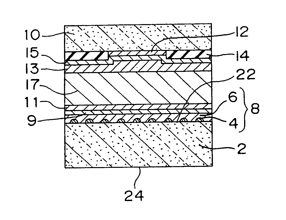
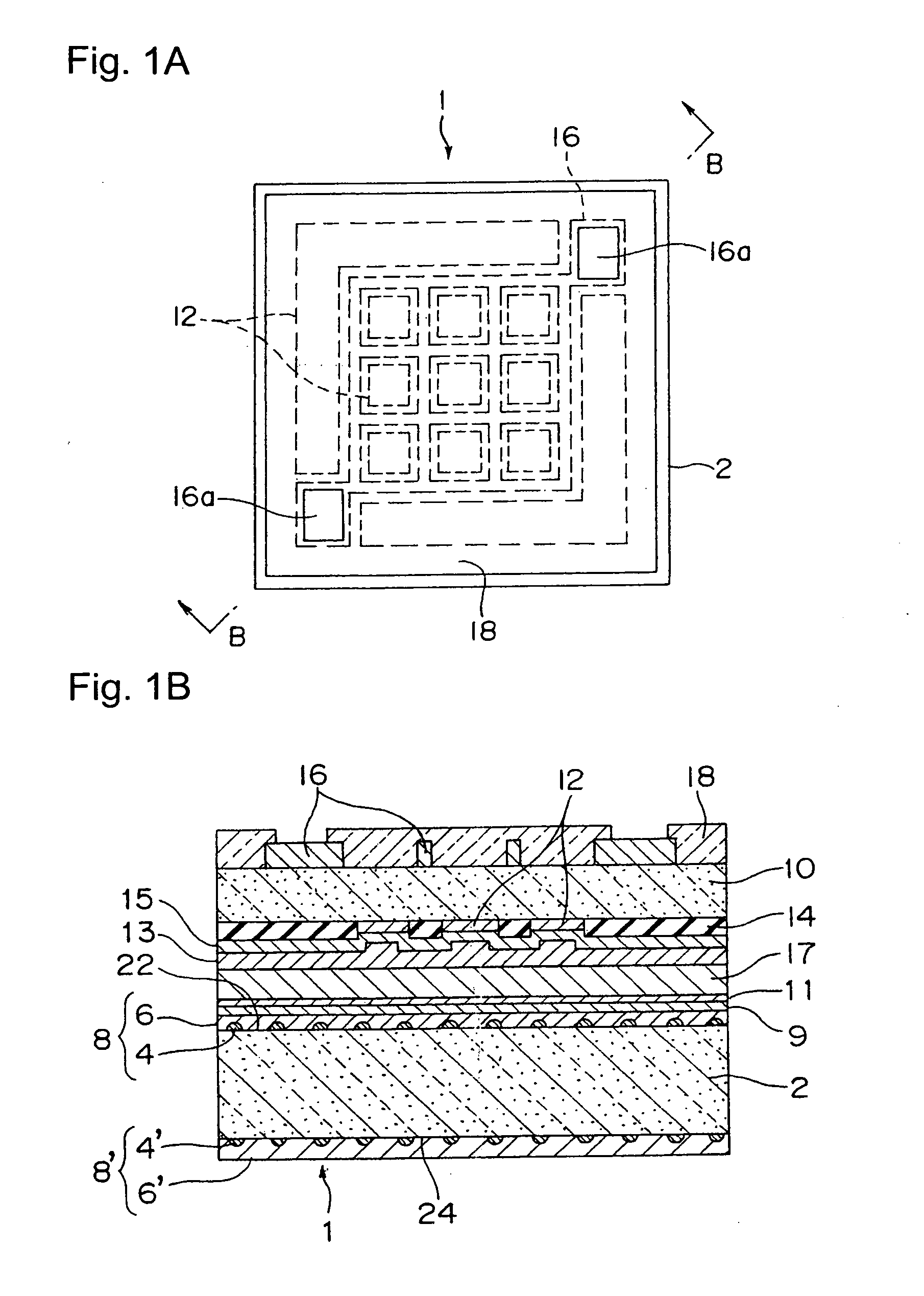
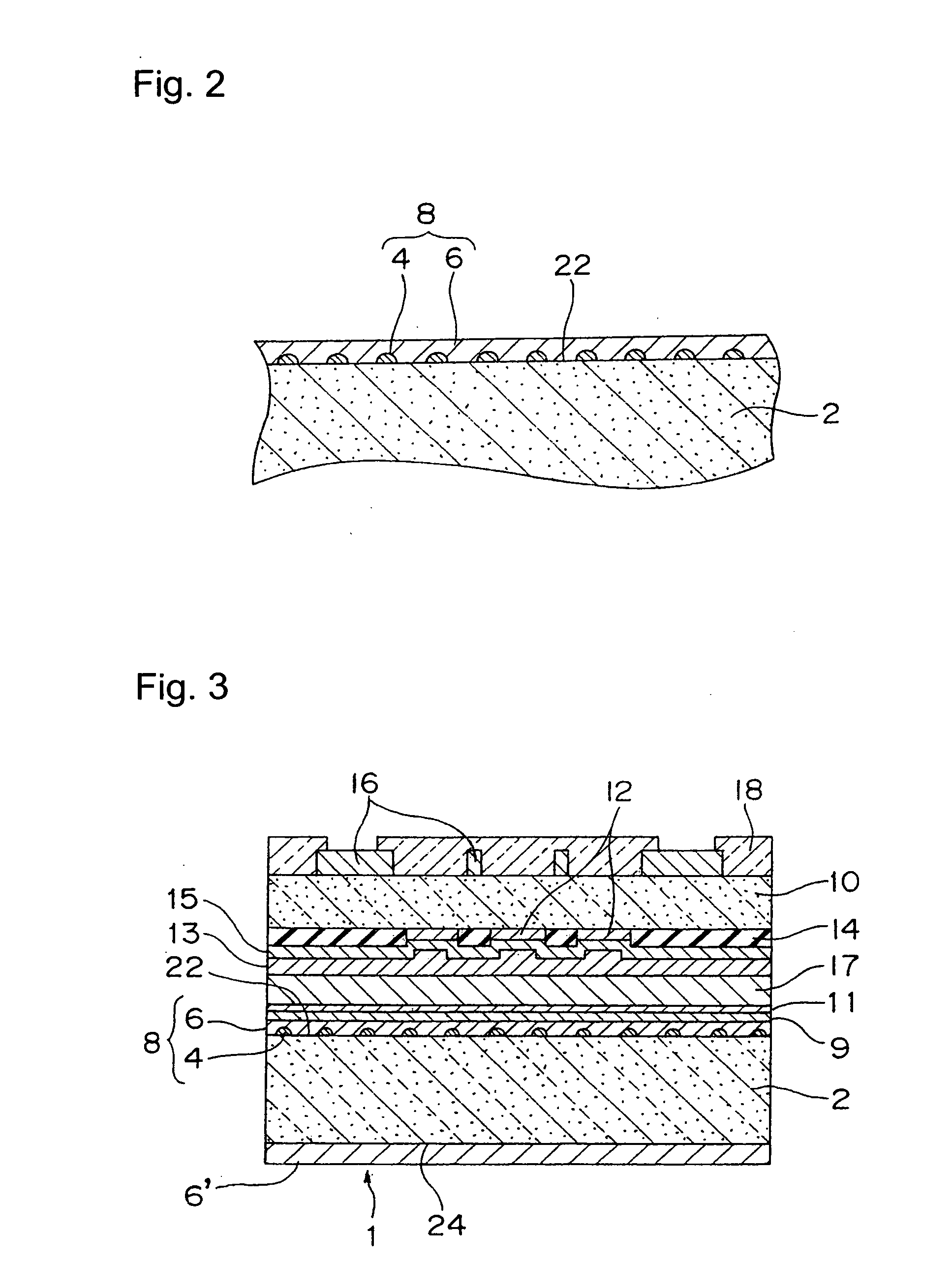
[0107]In the present example, the present invention is applied to a light emitting diode having an emission wavelength of 375 nm, and according to the method shown in FIGS. 5A to 5F, a nitride semiconductor device having a structure shown in FIGS. 1A and 1B is fabricated.

[0108](Growth Substrate)

[0109]A substrate made of sapphire (C-plane) was used as a growth substrate 20 and surface cleaning was carrier out at 1050° C. in hydrogen atmosphere in a MOOCVD reaction vessel.

[0110](Underlayer)

[0111]Buffer layer: Successively, a buffer layer of GaN of about 200 Å in thickness was grown on the substrate at 510° C. in hydrogen atmosphere by using ammonia and TMG (trimethylgallium).

[0112]High temperature grown layer: After the buffer layer was grown, only TMG was stopped and the temperature was raised to 1050° C., then a high temperature grown nitride semiconductor 4 of undoped GaN was grown to a thickness of 5 μm by using TMG and ammonia as source gases.

[0113](n-Type Cladding / Contact Layer)...

example 2

[0137]A nitride semiconductor device is formed in a similar manner as in Example 1, except that the first metal layer is NiSi2. The nitride semiconductor device having significantly excellent adhesion between the silicon substrate and the metal electrodes 8,8′ is obtained similarly as in Example 1.

example 3

[0138]A nitride semiconductor device is formed in a similar manner as in Example 1, except that the p-type silicon substrate is used in place of the n-type silicon substrate and the second metal layer 6 is Ti. The nitride semiconductor device having significantly excellent adhesion between the silicon substrate and the metal electrodes 8,8′ is obtained similarly as in Example 1.


PUM

PropertyMeasurementUnit
thicknessaaaaaaaaaa
resistivityaaaaaaaaaa

Abstract

In the nitride semiconductor device using the silicon substrate, the metal electrode formed on the silicon substrate has both ohmic contact property and adhesion, so that the nitride semiconductor device having excellent electric properties and reliability is obtained. The nitride semiconductor device includes a silicon substrate (2), a nitride semiconductor layer (10) formed on the silicon substrate (2), and metal electrodes (8, 8′) formed in contact with the silicon substrate (2). The metal electrodes (8, 8′) has first metal layers (4, 4′) which are formed in a shape of discrete islands and in contact with the silicon substrate (2), and second metal layers (6, 6′) which are in contact with the silicon substrate (2) exposed among the islands of the first metal layers (4, 4′) and are formed to cover the first metal layers (4, 4′). Further, the second metal layers (6, 6′) are made of a metal capable of forming ohmic contact with silicon, and the first metal layers (4, 4′) are made of an alloy containing a metal and silicon, in which the metal is different than that in the second metal layer (6,6′).

Description

BACKGROUND OF THE INVENTION[0001]1. Field of the Invention[0002]The present invention relates to a nitride semiconductor device using a silicon substrate and method of manufacturing the nitride semiconductor device, and more particularly, relates to a nitride semiconductor device having an electrode of excellent ohmic contact properties and adhesion with respect to the silicon substrate and method of manufacturing the nitride semiconductor device.[0003]2. Description of the Related Art[0004]A nitride semiconductor device is capable of producing high-output, short-wavelength light and has widely been used for a blue or green LED and for a white LED, in which a fluorescent material is used in combination of a nitride semiconductor device. In addition, a nitride semiconductor device has been intensively studied also as a high-speed electric device such as HEMT.[0005]When manufacturing a nitride semiconductor device, a nitride semiconductor layer is generally grown by hetero-epitaxial g...

Claims


Application Information

Patent Timeline
Patent Type & Authority Applications(United States)
IPC IPC(8): H01L21/28H01L29/06
CPCH01L21/6835H01L21/743H01L33/0079H01L33/32H01L21/28017H01L33/387H01L33/40H01L2221/6835H01L2933/0016H01L33/38H01L33/0093
Inventor WATANABE, KENTAROMINATO, SHUNSUKEMARUTSUKI, GIICHI
Owner NICHIA CORP
Why Eureka
Try Eureka