

GaAs semiconductor substrate and fabrication method thereof
a technology of semiconductor substrate and fabrication method, which is applied in the direction of crystal growth process, semiconductor/solid-state device details, after-treatment details, etc., can solve the problem of degrading the property of the semiconductor devi
- Summary
- Abstract
- Description
- Claims
- Application Information
AI Technical Summary
Benefits of technology
Problems solved by technology
Method used
Image

Examples
first embodiment
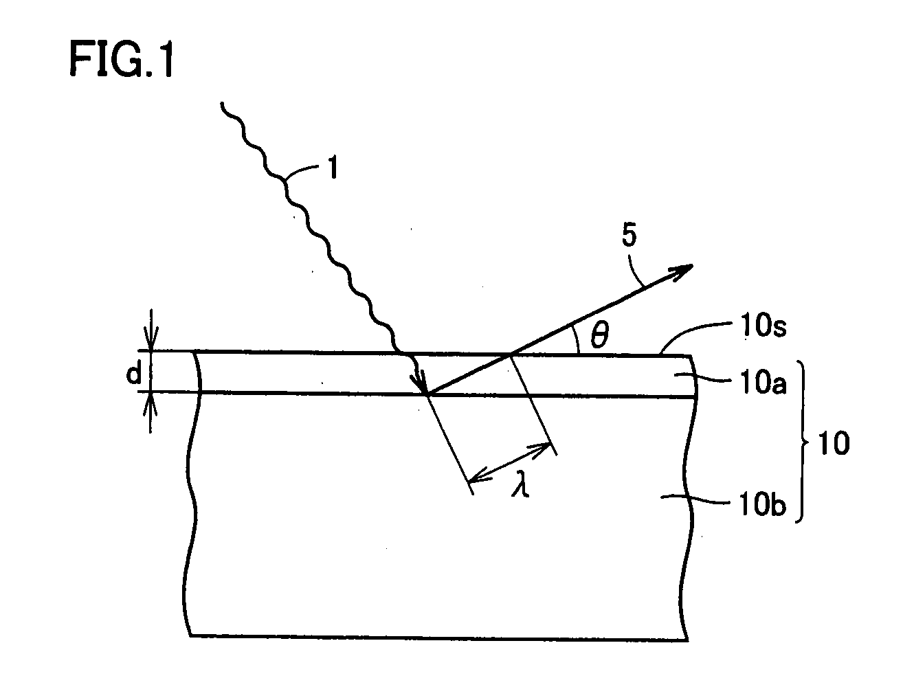
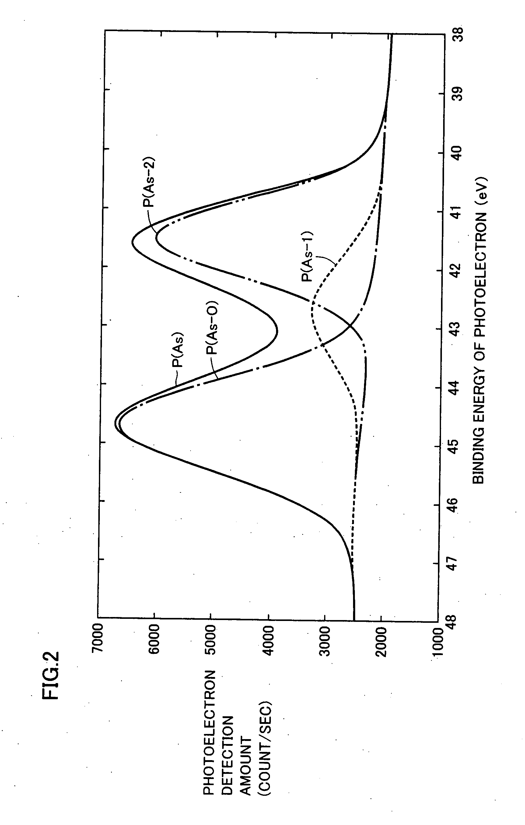
[0023]An embodiment of a GaAs semiconductor substrate of the present invention is directed to a GaAs semiconductor substrate 10 having a surface layer 10a, as shown in FIGS. 1-3. When the atomic ratio is calculated using a 3d electron spectrum of Ga atoms and As atoms measured under the condition of 10° for the photoelectron take-off angle θ by X-ray photoelectron spectroscopy (XPS), the structural atomic ratio of all Ga atoms to all As atoms (Ga) / (As) at the surface layer 10a is at least 0.5 and not more than 0.9, the ratio of As atoms bound with O atoms to all Ga atoms and all As atoms (As—O) / {(Ga)+(As)} at the surface layer 10a is at least 0.15 and not more than 0.35, and the ratio of Ga atoms bound with O atoms to all Ga atoms and all As atoms (Ga—O) / {(Ga)+(As)} at the surface layer 10a is at least 0.15 and not more than 0.35.
[0024]By setting the Ga / As ratio smaller as compared to the stoichiometric composition ratio (that is, (Ga) / (As)=1 / 1), formation of oxides on the substrate...
second embodiment
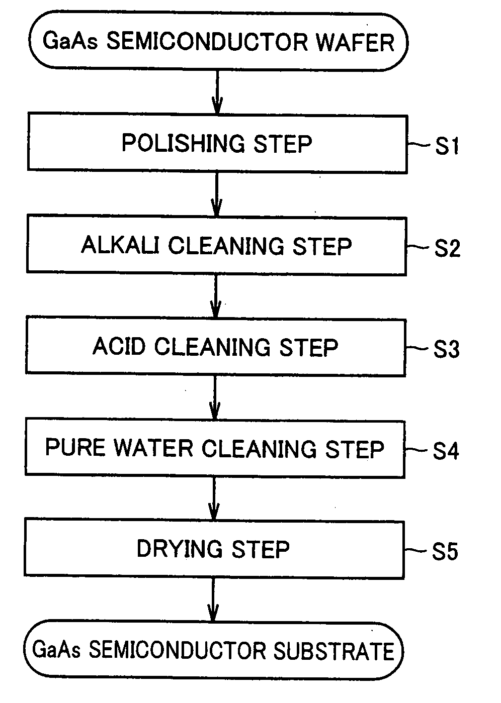
[0039]According to an embodiment of the present invention, a fabrication method of a GaAs semiconductor substrate includes, as shown in FIG. 4, a polishing step S1 of polishing the surface of a GaAs semiconductor wafer, an alkali cleaning step S2 of cleaning the polished surface with an alkali cleaning solution, and an acid cleaning step S3 of cleaning the surface subjected to alkali cleaning with an acid cleaning solution including 0.3 ppm to 0.5 mass % acid.
[0040]The foreign objects in the polished agent and / or impurities adhering to the surface of the semiconductor wafer in the polishing step can be removed by the alkali cleaning step. Further, the impurities in the alkali cleaning solution adhering to the surface of semiconductor wafer in the alkali cleaning step can be removed by the acid cleaning step. The ratio of Ga atoms and As atoms on the surface is rendered appropriate by selecting an acid of an appropriate concentration in the acid cleaning solution to suppress generati...
third embodiment
[0051]A fabrication method of a GaAs semiconductor substrate according to another embodiment of the present invention includes, as shown in FIG. 5, an alkali cleaning step (FIG. 5 (a)) of cleaning the polished surface of GaAs semiconductor wafer 11 first with an organic solvent such as alcohol, and then with an alkali cleaning solution 21, and an acid cleaning step (FIG. 5 (c)) of cleaning the alkali-cleaned surface with an acid cleaning solution 23 including 0.3 ppm to 0.5 mass % of acid. The present embodiment is directed to cleaning GaAs semiconductor wafer 11 in batch form, and further includes a first pure water cleaning step (FIG. 5 (b)) of cleaning the alkali-cleaned surface with pure water 25, between the alkali cleaning step and acid cleaning step, a second pure water cleaning step (FIG. 5 (d)) of cleaning the surface subjected to acid cleaning with pure water, after the acid cleaning step, and the step (FIG. 5 (e)) of drying the pure water remaining at the surface cleaned ...
PUM
| Property | Measurement | Unit |
|---|---|---|
| photoelectron take-off angle | aaaaa | aaaaa |
| surface roughness RMS | aaaaa | aaaaa |
| melting point | aaaaa | aaaaa |
Abstract
Description
Claims
Application Information