Method of Polishing Compound Semiconductor Substrate, Compound Semiconductor Substrate, Method of Manufacturing Compound Semiconductor Epitaxial Substrate, and Compound Semiconductor Epitaxial Substrate

a technology of compound semiconductor and epitaxial substrate, which is applied in the direction of manufacturing tools, lapping machines, instruments, etc., can solve the problems of excessively difficult post-polishing cleaning, oxide film formation on the wafer surface, and oxide film is left on the substrate surface, so as to reduce the amount of oxygen superficially present on the substrate

Active Publication Date: 2008-12-04
SUMITOMO ELECTRIC IND LTD
View PDF4 Cites 9 Cited by
  • Summary
  • Abstract
  • Description
  • Claims
  • Application Information

AI Technical Summary

Benefits of technology

[0012]Accordingly, an object of the present invention, brought about in order to resolve issues such as discussed above, is to make available a compound semiconductor-substrate polishing methods, compound semiconductor substrate, compound-semiconductor epitaxial-substrate manufacturing methods, and compound semiconductor epitaxial substrates, whereby oxygen superficially present on the substrates is reduced.

Problems solved by technology

An oxide film ends up being left on the substrate surface, however, because the chloroisocyanuric acid contained in the polishing agent is strongly oxidizing.
Moreover, clearing away the oxide film in the post-polishing stages leading up to the final cleaning process is exceedingly difficult.
However, because oxide-film buildup cannot be sufficiently cleared away with a surfactant, an oxide film forms thickly on the wafer surface.
However, the fact that the aqueous solution for stopping the polishing reactions contains an oxidant and the fact that the aqueous solution is employed post-polish mean that, with the oxidation reaction is not being halted, formation of oxide film on the substrate surface cannot be kept adequately under control.
A consequent problem is that the number of electrons that reach the active layers drops, adversely affecting the device properties.
A further problem is that a heavy presence of oxide film on the compound semiconductor substrate worsens the morphology of (the growth striations and defects in) epitaxial layers built onto the oxide film.

Method used


Image

  • Method of Polishing Compound Semiconductor Substrate, Compound Semiconductor Substrate, Method of Manufacturing Compound Semiconductor Epitaxial Substrate, and Compound Semiconductor Epitaxial Substrate
  • Method of Polishing Compound Semiconductor Substrate, Compound Semiconductor Substrate, Method of Manufacturing Compound Semiconductor Epitaxial Substrate, and Compound Semiconductor Epitaxial Substrate
  • Method of Polishing Compound Semiconductor Substrate, Compound Semiconductor Substrate, Method of Manufacturing Compound Semiconductor Epitaxial Substrate, and Compound Semiconductor Epitaxial Substrate

Examples


embodiment mode 1

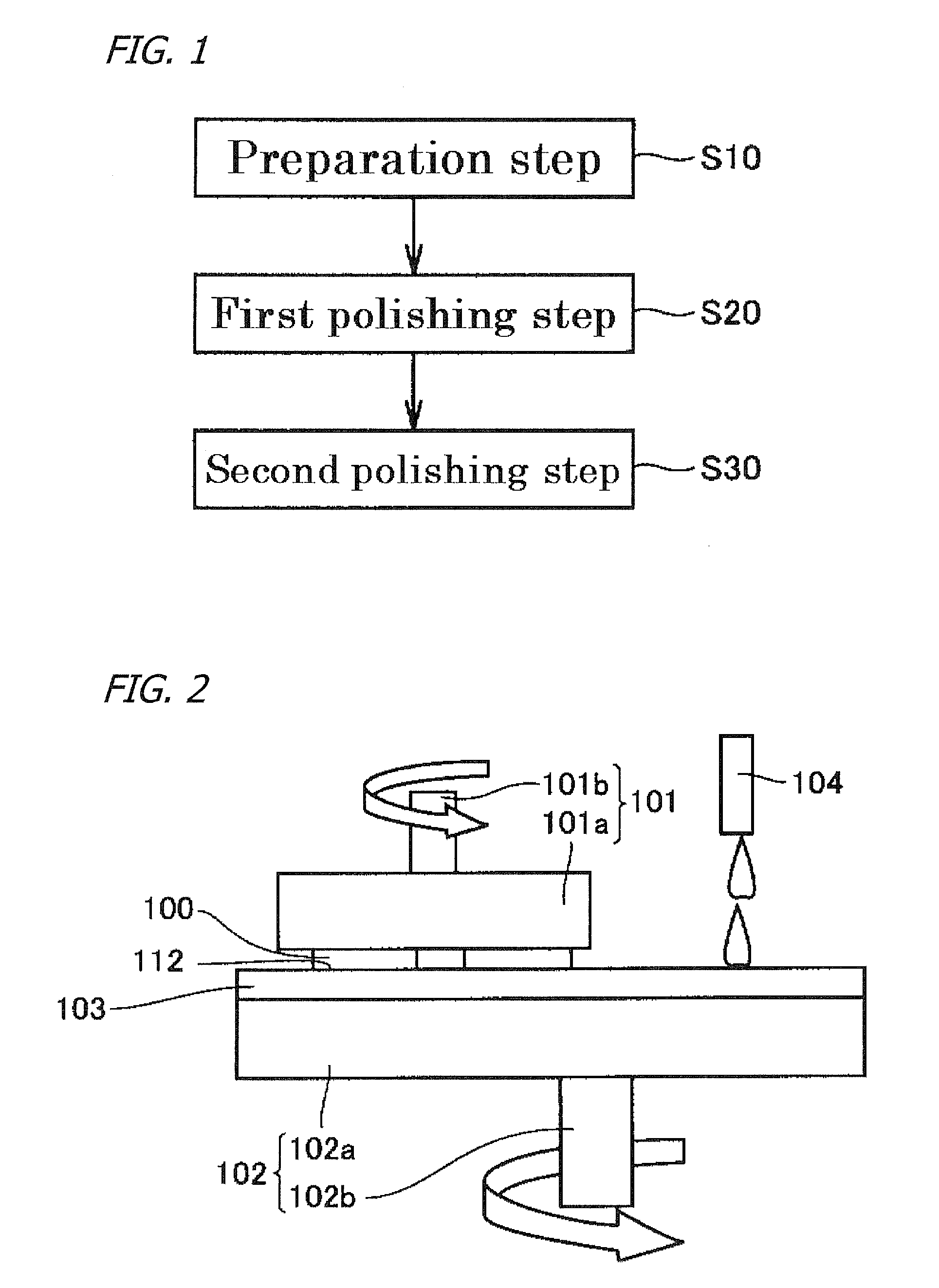
[0045]FIG. 1 is a flow chart representing a method of polishing a compound semiconductor substrate in Embodiment Mode 1 of the present invention. With reference to FIG. 1, an explanation of the compound semiconductor substrate polishing method will be made.

[0046]First, as represented in FIG. 1, a preparation step (S10) is carried out, in which a compound semiconductor substrate is prepared. In the preparation step (S10), the compound semiconductor substrate composed of gallium arsenide, indium phosphorus, indium antimony, gallium antimony, indium arsenide, gallium nitride, indium nitride, and aluminum nitride is preferably prepared. It should be understood that the compound semiconductor substrate to be prepared may be a bulk crystal or a thin film formed on a substrate composed of, for example, the bulk crystal.

[0047]Next, as represented in FIG. 1, a first polishing step (S20) is carried out, in which the compound semiconductor substrate is polished with a chloric polishing agent. ...

embodiment mode 2

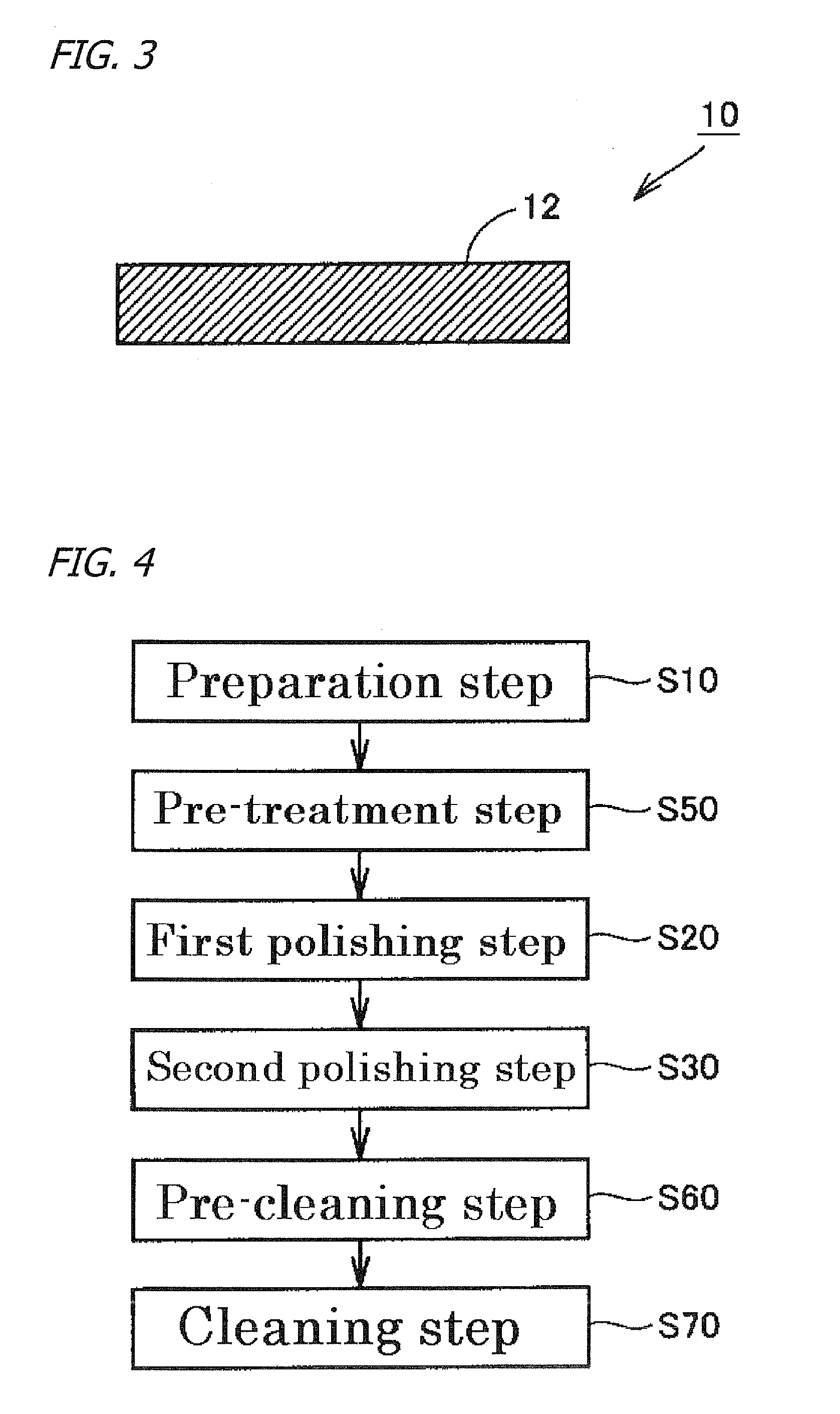
[0067]FIG. 4 is a flow chart representing a method of surface treating the compound semiconductor substrate in Embodiment Mode 2 of the present invention. Referring to FIG. 4, the compound semiconductor-substrate surface treating method in Embodiment Mode 2 of the present invention will be described. As represented in FIG. 4, the compound semiconductor-substrate surface treating method in Embodiment Mode 2 has steps similar to those of the compound semiconductor-substrate polishing method in Embodiment Mode 1, but differs only in comprising a pre-treatment step (S50), pre-cleaning step (S60), and a cleaning step (S70).

[0068]First, as illustrated in FIG. 4, the preparation step (S10) of preparing the compound semiconductor substrate is carried out as in Embodiment Mode 1.

[0069]Next, prior to the first and second polishing steps (S20, S30), pre-treatment step (S50) is carried out, in which the compound semiconductor substrate is polished. In the pre-treatment step (S50), before the fi...

embodiment mode 3

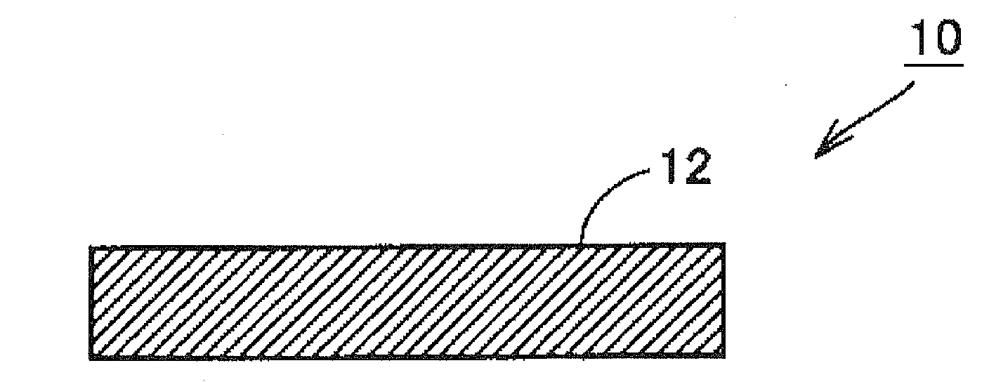
[0078]FIG. 6 is a flow chart representing a compound semiconductor epitaxial-substrate manufacturing method of the Embodiment Mode 3 of the present invention. Referring to FIG. 6, the compound semiconductor epitaxial-substrate manufacturing method will be described. The compound semiconductor epitaxial-substrate manufacturing method comprises basically steps similar to those of the compound semiconductor substrate polishing method in Embodiment Mode 1, but differs only in carrying out the post-treatment step (S40) of forming on the front side 12 of the compound semiconductor substrate 10 an epitaxial layer 21.

[0079]Specifically, first, as illustrated in FIG. 6, the compound semiconductor substrate polishing method (S10 to S30) is carried out.

[0080]Next, the post-treatment step (S40) is carried out, in which the epitaxial layer is formed on the front side of the compound semiconductor substrate 10. It should be understood that the compound semiconductor substrate used in the post-tre...


PUM

PropertyMeasurementUnit
pHaaaaaaaaaa
RMS roughnessaaaaaaaaaa

Abstract

Compound-semiconductor-substrate polishing methods, compound semiconductor substrates, compound-semiconductor-epitaxial-substrate manufacturing methods, and compound semiconductor epitaxial substrates whereby oxygen superficially present on the substrates reduced. A compound semiconductor-substrate polishing method includes a preparation step (S10), a first polishing step (S20), and a second polishing step (S30). In the preparation step (S10), a compound semiconductor substrate is prepared. In the first polishing step (S20), the compound semiconductor substrate is polished with a chloric polishing agent. In the second polishing step (S30), subsequent to the first polishing step (S20), a polishing operation utilizing an alkaline aqueous solution containing an inorganic builder and having pH of 8.5 to 13.0 inclusive is performed.

Description

BACKGROUND OF THE INVENTION[0001]1. Technical Field[0002]The present invention relates to methods of polishing compound semiconductor substrates, to the compound semiconductor substrates, to methods of manufacturing compound semiconductor epitaxial substrates, and to the compound semiconductor epitaxial substrates; more particularly the invention relates to compound-semiconductor-substrate polishing methods that reduce oxygen superficially present on the substrate, to the compound semiconductor substrates, to compound-semiconductor epitaxial-substrate manufacturing methods, and to the compound semiconductor epitaxial substrates.[0003]2. Description of the Related Art[0004]Compound semiconductor substrates have been widely used for semiconductor lasers, light emitting diodes (LEDs), and high-speed devices because they have luminescent properties and high electron mobility. Ordinarily, in compound-semiconductor-substrate manufacturing procedures polish is carried out. Methods of polis...

Claims


Application Information

Patent Timeline
Patent Type & Authority Applications(United States)
IPC IPC(8): B32B3/00B32B15/04B24B37/00H01L21/304
CPCB24B37/0056B24B37/042Y10T428/24355H01L21/02052H01L21/02024Y10T428/31678
Inventor MEZAKI, YOSHIONISHIURA, TAKAYUKINAKAYAMA, MASAHIRO
Owner SUMITOMO ELECTRIC IND LTD
Why Eureka
Try Eureka