

Microlitographic projection exposure apparatus and immersion liquid therefore
a technology of exposure apparatus and exposure liquid, which is applied in the direction of microlithography exposure apparatus, printers, instruments, etc., can solve the problems of affecting the durability of the equipment, affecting the quality of the image, so as to reduce the chemical reactivity of the equipmen
- Summary
- Abstract
- Description
- Claims
- Application Information
AI Technical Summary
Benefits of technology
Problems solved by technology
Method used
Image

Examples
Embodiment Construction
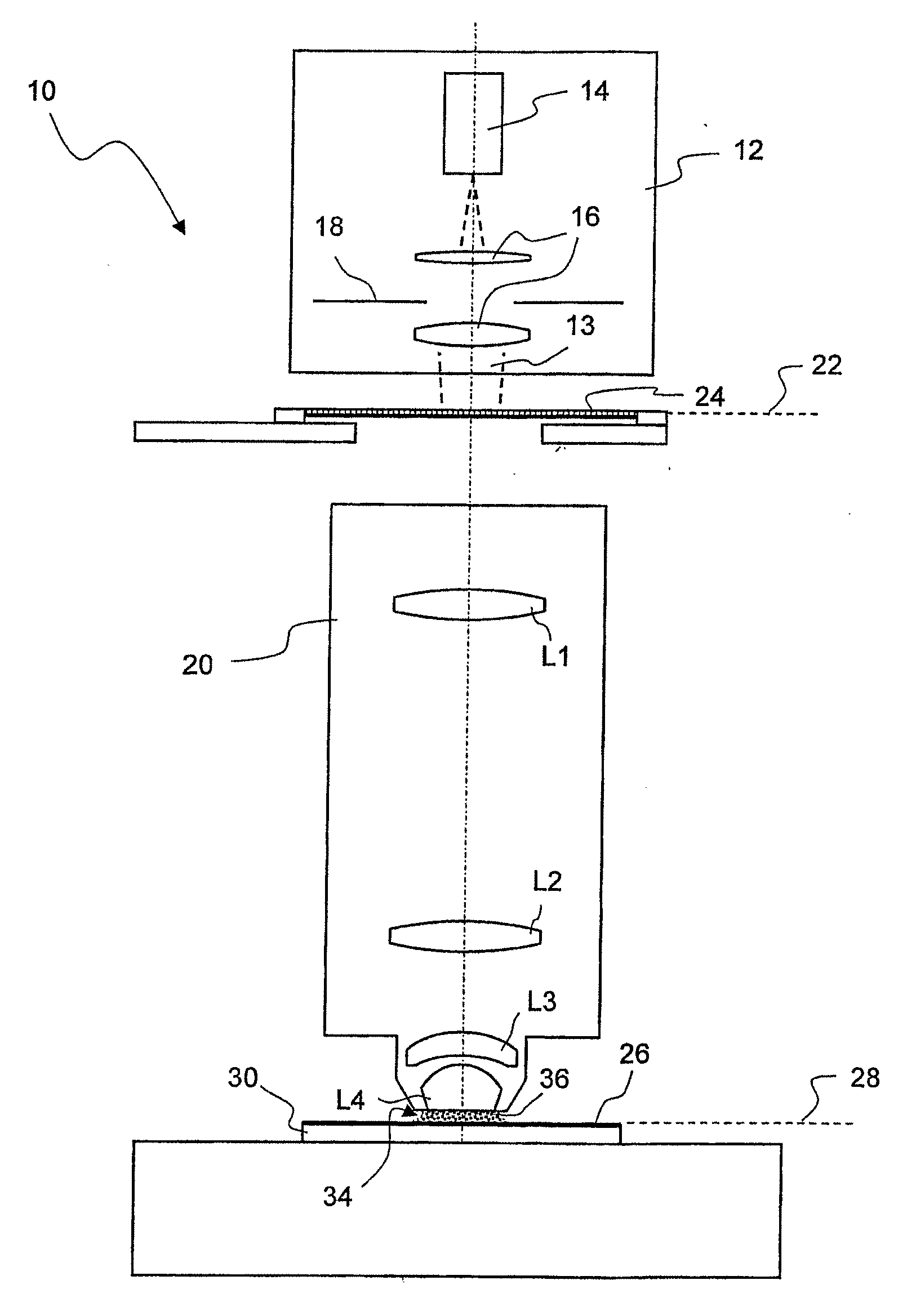
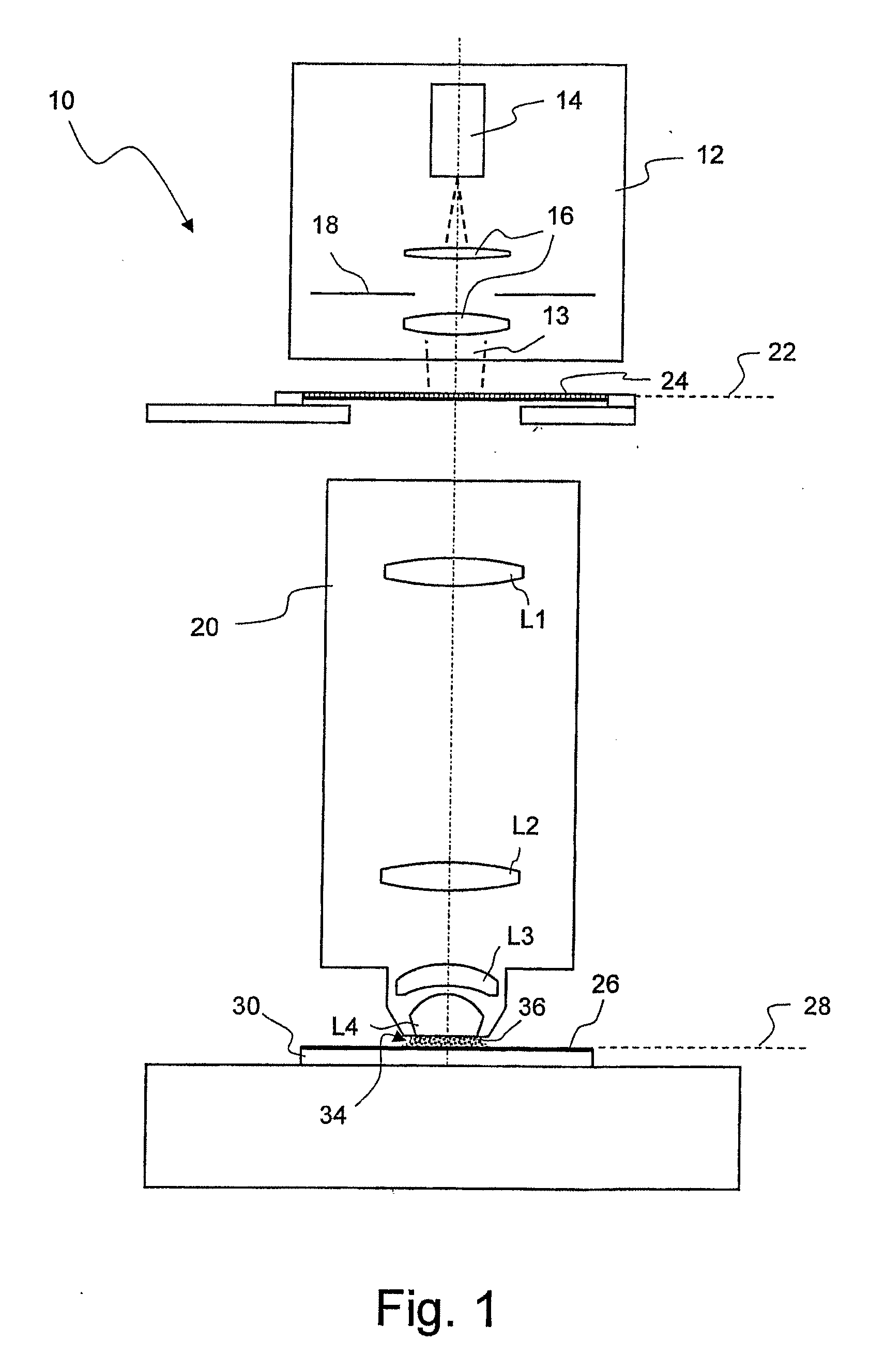
[0054]FIG. 1 shows a meridian section through a microlithographic projection exposure apparatus, denoted overall by 10, according to a first exemplary embodiment of the invention in a highly simplified schematic representation. The projection exposure apparatus 10 has an illumination device 12 for the generation of projection light 13, which inter alia comprises a light source 14, illumination optics indicated by 16 and a diaphragm 18. In the exemplary embodiment which is represented, the projection light has a wavelength of 193 nm.
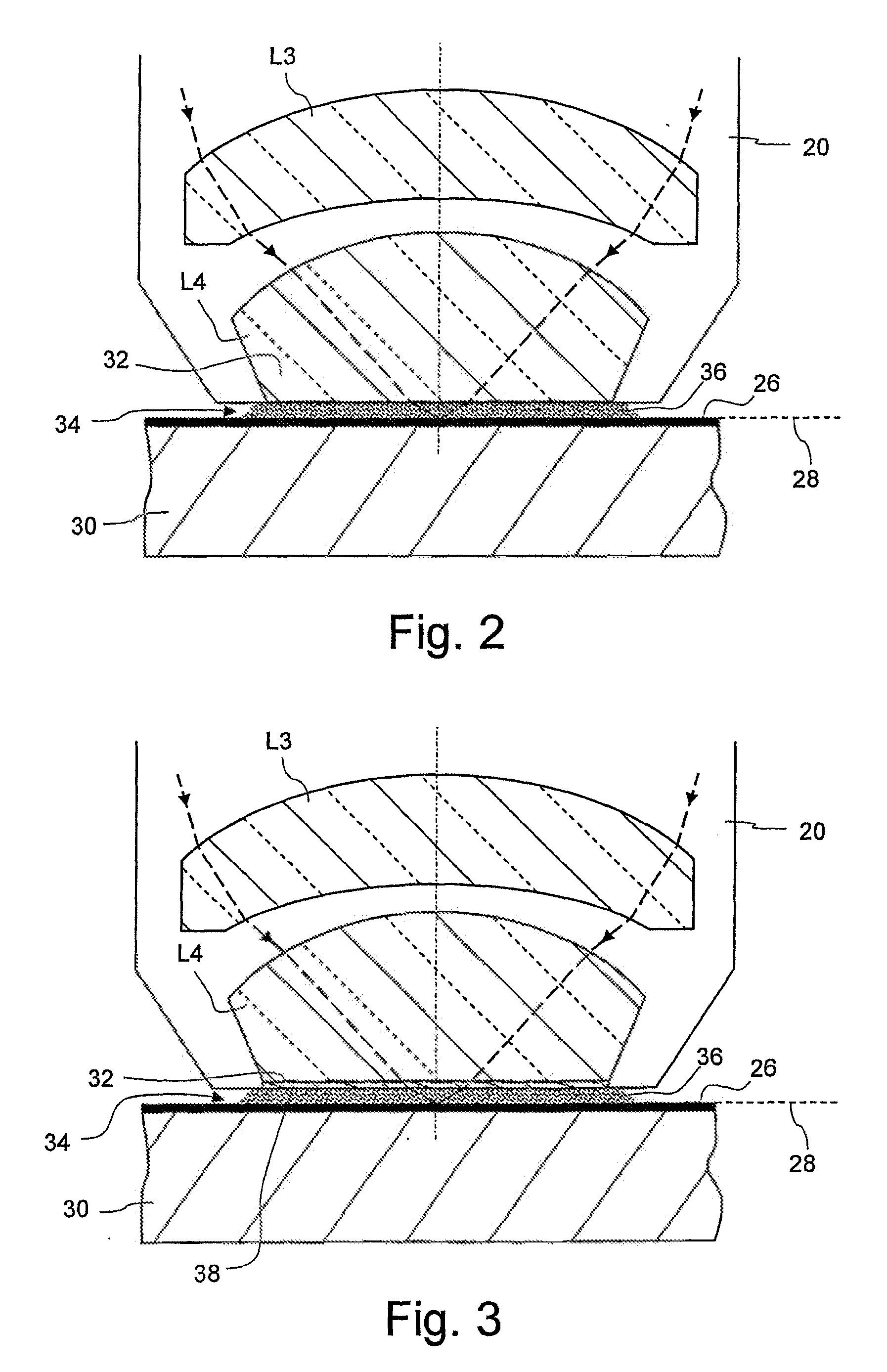
[0055]The projection exposure apparatus 10 furthermore includes a projection lens 20 which contains a multiplicity of lens elements, only some of which denoted by L1 to L4 are represented by way of example in FIG. 1 for the sake of clarity. The projection lens 20 is used to project a reduced image of a reticle 24, which is arranged in an object plane 22 of the projection lens 20, onto a photosensitive layer 26 which is arranged in an image plane 28 of the...
PUM
| Property | Measurement | Unit |
|---|---|---|
| wavelengths | aaaaa | aaaaa |
| wavelengths | aaaaa | aaaaa |
| pressure | aaaaa | aaaaa |
Abstract
Description
Claims
Application Information