Light emitting diode having active region of multi quantum well structure

a light-emitting diode and active region technology, applied in the field of light-emitting diodes, can solve the problems of reducing the luminous efficiency of led, dislocation, cracking or warpage of semiconductor layers, etc., and achieves the effect of improving the luminous efficiency and increasing the recombination rate of electrons and holes

Active Publication Date: 2008-12-18
SEOUL VIOSYS CO LTD
View PDF1 Cites 60 Cited by
  • Summary
  • Abstract
  • Description
  • Claims
  • Application Information

AI Technical Summary

Benefits of technology

[0020]This invention provides an LED with improved luminous efficiency by increasing recombination rate of electrons and holes.

Problems solved by technology

However, if a Group III element nitride semiconductor layer is grown on the heterogeneous substrate 11, a crack or warpage occurs in the semiconductor layer and dislocation is produced due to the difference of lattice coefficients and thermal expansion coefficients between the semiconductor layer and the substrate.
Such crystal defects cause non-light emitting recombination, thereby decreasing luminous efficiency of the LED.
However, since the lattice mismatch between the uppermost well layer 19a and the P-type clad layer 21 is more increased than that between the barrier layer 19b and the P-type clad layer 21, crystal defects in the vicinity of the P-type clad layer 21 are increased, and therefore, increasing the luminous efficiency is difficult.
The excessive occurrence of such carrier overflow causes the recombination rate of electrons and holes to deteriorate, thereby decreasing luminous efficiency.

Method used


Image

  • Light emitting diode having active region of multi quantum well structure
  • Light emitting diode having active region of multi quantum well structure
  • Light emitting diode having active region of multi quantum well structure

Examples


first embodiment

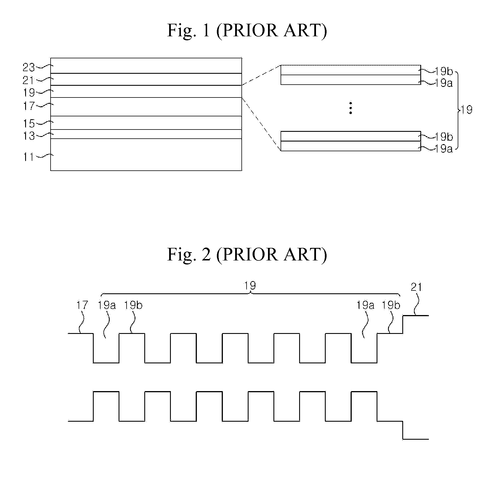
[0083]FIG. 7 is a band diagram illustrating an active region of a multi quantum well structure according to a modification of the present invention.

[0084]Referring FIG. 7, a middle barrier layer 59c having a bandgap relatively wider than the first and n-th barrier layers 59b-1 and 59b-n is positioned therebetween as described with reference to FIG. 6. In addition thereto, other middle barrier layer 59c′ having a bandgap relatively wider than the first and n-th barrier layers 59b-1 and 59b-n is positioned therebetween. The other middle barrier layer 59c′ may be positioned between the first barrier layer 59b-1 and the middle barrier layer 59c.

[0085]Like the middle barrier layer 59c, the other middle barrier layer 59c′ has a relatively wide bandgap and therefore restricts the movement of electrons. Particularly, if the other middle barrier layer 59c′ is disposed close to the middle barrier layer 59c, the recombination rate of electrons and holes is more increased. In addition, as show...

second embodiment

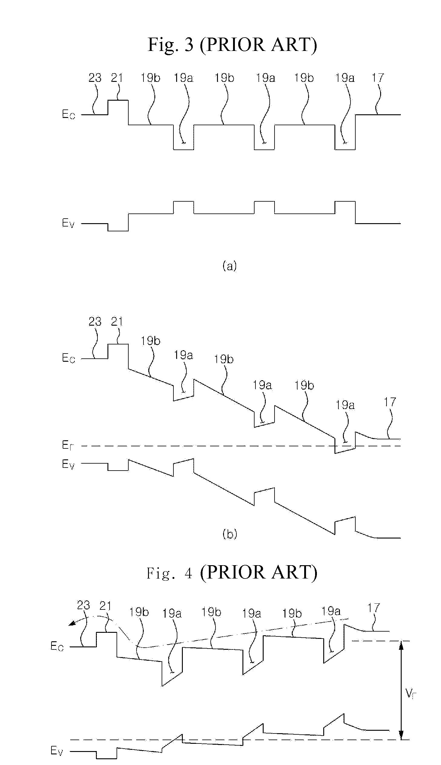
[0100]However, in the LED according to the present invention, since the barrier layer 79b close to the N-type compound semiconductor layer 57 has a narrower bandgap than the barrier layer 79d close to the P-type compound semiconductor layer 63, the band slope of the barrier layers may be decreased even though a high forward voltage is applied to the LED. Particularly, if a forward voltage is applied to the LED, the bandgap of the barrier layers 79b, 79c and 79d can be controlled so that the conduction bands of the barrier layers are positioned at the generally same energy level. Accordingly, removing the driving force inducing carrier overflow in the active region 79 and improving the recombination rate of electrons and holes are possible.

[0101]Although the three barrier layers 79b, 79c and 79d have been shown and described in the second embodiment of the present invention, the present invention is not limited thereto. That is, a larger number of the barrier layers may be alternatel...

third embodiment

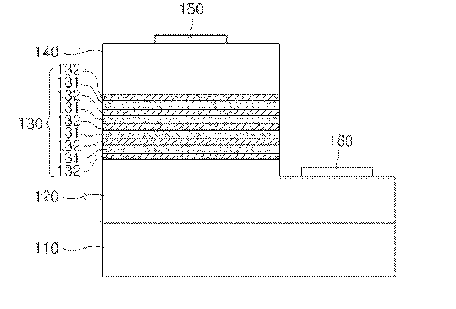
[0104]FIG. 13 is a sectional view illustrating an LED having an active region of a multi quantum well structure according to the present invention. The LED according to this embodiment has the generally same laminated structure as the LED described with reference to FIG. 5, which will be described in brief. Only the differences will be described in detail.

[0105]Referring to FIG. 13, an N-type semiconductor layer 120, an active region 130 and a P-type semiconductor layer 140 are laminated and formed on a substrate 110. A P-electrode 150 is formed on the P-type semiconductor layer 140. After a predetermined region of the N-type semiconductor layer 120 is exposed through a mesa etching process, an N-electrode 160 is formed on the exposed N-type semiconductor layer 120.

[0106]The active region 130 is formed to have a multiple quantum well structure by alternately laminating well layers 131 having a narrow energy bandgap and barrier layers 132 having an energy bandgap wider than the well ...


PUM


Abstract

Disclosed is a light emitting diode (LED) having an active region of a multiple quantum well structure in which well layers and barrier layers are alternately laminated between a GaN-based N-type compound semiconductor layer and a GaN-based P-type compound semiconductor layer. The LED includes a middle barrier layer having a bandgap relatively wider than the first barrier layer adjacent to the N-type compound semiconductor layer and the n-th barrier layer adjacent to the P-type compound semiconductor layer. The middle barrier layer is positioned between the first and n-th barrier layers. Accordingly, positions at which electrons and holes are combined in the multiple quantum well structure to emit light can be controlled, and luminous efficiency can be enhanced. Furthermore, an LED is provided with enhanced luminous efficiency using a bandgap engineering or impurity doping technique.

Description

CROSS REFERENCE TO RELATED APPLICATIONS[0001]This application claims priority from and the benefit of Korean Patent Application No. 10-2007-0057260, filed on Jun. 12, 2007, Korean Patent Application No. 10-2007-0062465, filed on Jun. 25, 2007, and Korean Patent Application No. 10-2007-0076477, filed on Jul. 30, 2007, all of which are hereby incorporated by reference for all purposes as if fully set forth herein.BACKGROUND OF THE INVENTION[0002]1. Field of the Invention[0003]The present invention relates to a light emitting diode, and more particularly, to a light emitting diode having an active region of a multi quantum well structure.[0004]2. Discussion of the Background[0005]In general, since Group III element nitrides, such as GaN, AlN and InGaN, have excellent thermal stability and a direct transition type energy band structure, they have recently come into the spotlight as materials for light emitting diodes (LEDs) in blue and ultraviolet regions. Particularly, an InGaN compoun...

Claims


Application Information

Patent Timeline
Patent Type & Authority Applications(United States)
IPC IPC(8): H01L33/00H01L33/16H01L33/06H01L33/20H01L33/32
CPCH01L33/32H01L33/06
Inventor LEE, DONG SEONKIM, GYU BEOM
Owner SEOUL VIOSYS CO LTD
Why Eureka
Try Eureka