GaN SUBSTRATE, SUBSTRATE WITH EPITAXIAL LAYER, SEMICONDUCTOR DEVICE, AND METHOD OF MANUFACTURING GaN SUBSTRATE

a technology of epitaxial layer and substrate, which is applied in the direction of polycrystalline material growth, chemically reactive gas growth, crystal growth process, etc., can solve the problem of lowering the luminance efficiency of led, and achieve the effect of improving luminance efficiency, stab manufacturing, and improving operating li

Inactive Publication Date: 2008-12-18
SUMITOMO ELECTRIC IND LTD
View PDF4 Cites 57 Cited by
  • Summary
  • Abstract
  • Description
  • Claims
  • Application Information

AI Technical Summary

Benefits of technology

[0008]It is an object of the present invention to provide a GaN substrate having a large diameter of 2 inches or more to industrially provide a semiconductor device such as a light emitting element with improved characteristics such as luminance efficiency, an operating life and the like at low cost, a substrate having an epitaxial layer formed on a main surface of the GaN substrate, a semiconductor device, and a method of manufacturing the GaN substrate.
[0009]The inventors have produced a GaN substrate having various off-angles in which a defect concentrated region is formed and a defect density is reduced in a region other than the defect concentrated region, based on the above manufacturing methods of a GaN substrate shown in Patent Document 1 and Patent Document 2, and made a prototype LED by forming an epitaxial layer on the main surface of the GaN substrate, and examined its characteristics. As a result, when a plane direction [0001] is inclined in one plane direction (one off-angle direction) with respect to the normal vector of the main surface, the crystal plane exposed to the surface of the GaN substrate can be a semipolar plane. Also, when the plane direction [0001] is further inclined in another plane direction (another off-angle direction), it has been found that variation in wavelength distribution in the main surface of the GaN substrate can be controlled (reduced). That is, a GaN substrate according to the present invention has a main surface and includes a low-defect crystal region and a defect concentrated region adjacent to the low-defect crystal region. The low-defect crystal region and the defect concentrated region extend from the main surface to a back surface positioned on the opposite side of the main surface. A plane direction [0001] is inclined in an off-angle direction with respect to a normal vector of the main surface.
[0010]Thus, when the plane direction (Miller Index) [0001] is inclined in the first off-angle direction, the main surface of the GaN substrate having the low-defect crystal region becomes a semipolar plane, and an epitaxial layer can be formed on the main surface. Therefore, as compared with the case where a light emitting element such as an LED is manufactured by forming an epitaxial layer on a polar plane of the (0001) plane of the GaN substrate, characteristics such as an operating life can be improved, the luminance efficiency of a light emitting element having an emission wavelength contained in a long-wavelength region of 500 nm or more is improved, and a wavelength shift amount due to change in an applied current amount can be reduced. As a result, when the above GaN substrate is used, a semiconductor device such as a light emitting element having excellent characteristics can be manufactured stably.

Problems solved by technology

Since the (0001) plane of the above GaN substrate, for example, is a polar plane, there has been a problem that the luminance efficiency of the LED is lowered in a long-wavelength region having an emission wavelength of 500 nm or more.

Method used


Image

  • GaN SUBSTRATE, SUBSTRATE WITH EPITAXIAL LAYER, SEMICONDUCTOR DEVICE, AND METHOD OF MANUFACTURING GaN SUBSTRATE
  • GaN SUBSTRATE, SUBSTRATE WITH EPITAXIAL LAYER, SEMICONDUCTOR DEVICE, AND METHOD OF MANUFACTURING GaN SUBSTRATE
  • GaN SUBSTRATE, SUBSTRATE WITH EPITAXIAL LAYER, SEMICONDUCTOR DEVICE, AND METHOD OF MANUFACTURING GaN SUBSTRATE

Examples


example 1

[0088]In order to confirm the effect of the present invention, the following experiments were performed. That is, a GaN substrate according to the present invention was manufactured, and a light emitting element was manufactured with the GaN substrate. Then, a relation between the wavelength of the emitted light and the supplied current amount in each of the GaN substrate and the light emitting element was measured as will be described later. In addition, for comparison, a GaN substrate in which the main surface is a c-plane and a GaN substrate in which the main surface is an m-plane were prepared, and light emitting elements were formed with the GaN substrates likewise for comparison. Thus, the characteristics of the light emitting elements as comparison examples were measured similarly. The contents of the experiment will be specifically described below.

(1) Preparation of GaN Substrate

(1-1) Preparation of GaN Substrate According to the Present Invention

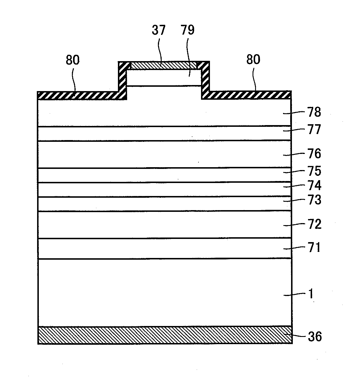
[0089]Base substrate:

[0090]A...

example 2

[0112]In order to confirm the effect of the present invention, the following experiments were performed. That is, GaN substrates were manufactured as samples ID1 to 66 according to an Example and samples ID11 to 5 according to a comparison example as will be described later, and the off-angle directions, the off-angles, the in-plane distribution of the off-angles, and the dislocation density of the samples of the GaN substrates were measured. Furthermore, a light emitting element was formed with each of the GaN substrates, and the change amount of the emission wavelength (blue shift: Δλ), the increase amount of the operation voltage (ΔVop) after 1000 hours and emission wavelength distribution (σ) in the plane of the GaN substrate were measured while the current value applied to the light emitting element was changed. The contents of the experiment will be described in more detail.

(1) Preparation of GaN Substrate

[0113]For all the samples (samples ID1 to 66 in the Example and samples ...

example 3

[0149]The following measurement was made on the GaN substrate according to the present invention.

(1) Preparation of GaN Substrate

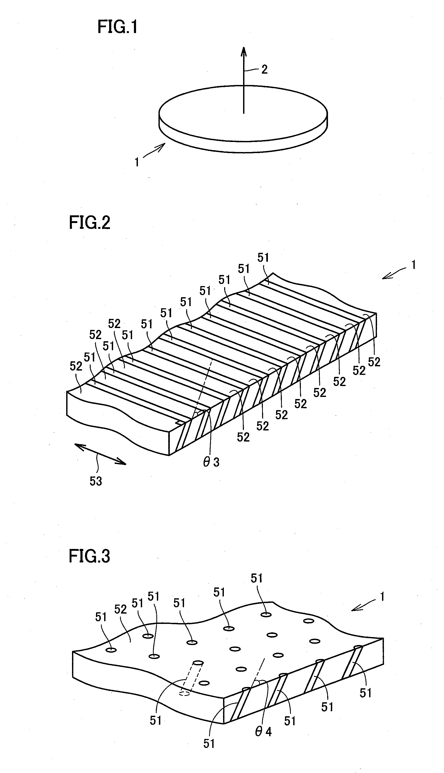
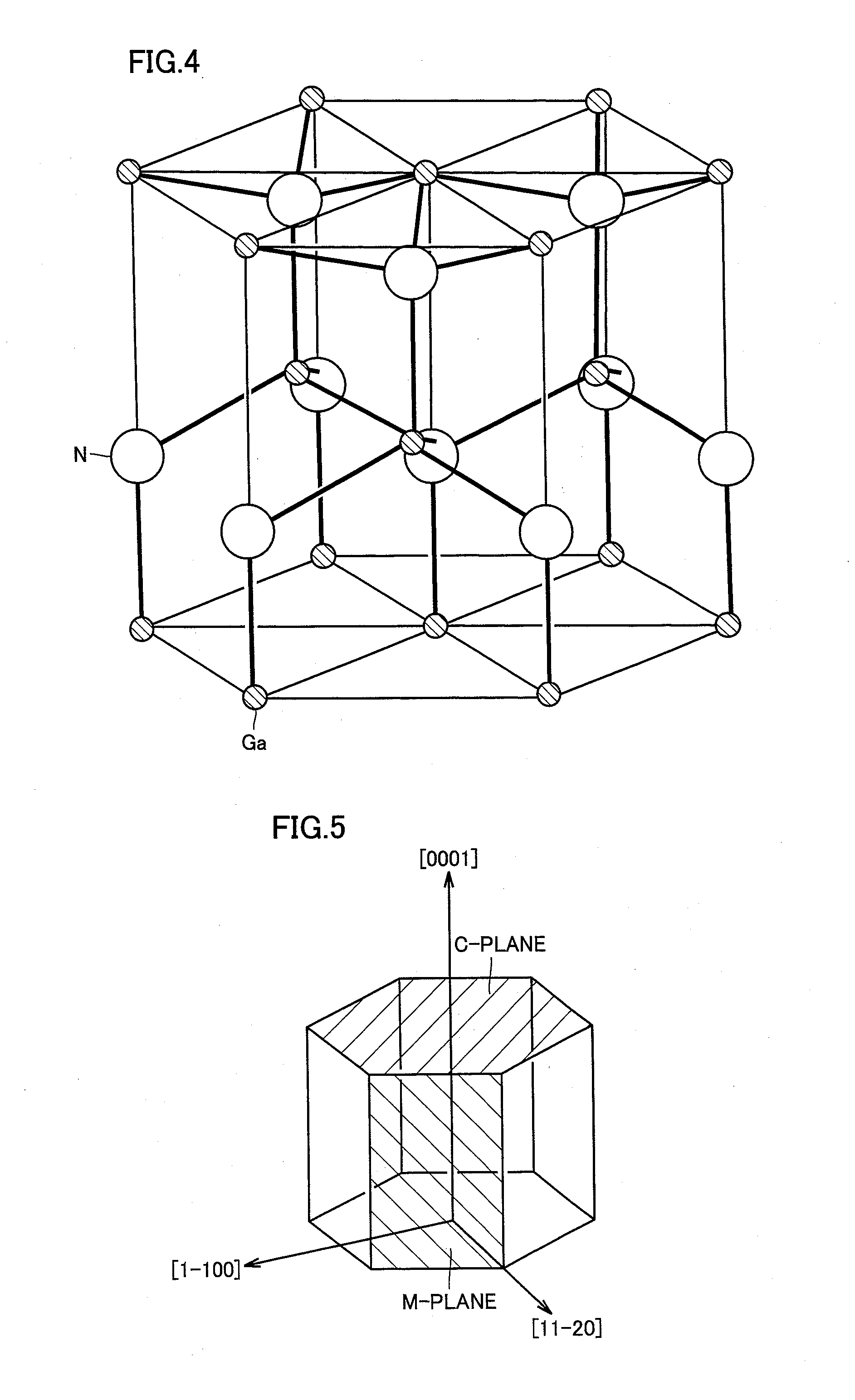
[0150]The GaN substrates of samples ID25 and ID41 of the Example were prepared. The manufacturing method of the GaN substrate was the same as that shown in Example 2. In addition, in the GaN substrate of sample ID25, the off-angle θ1 in [11-20] direction of the base substrate (GaAs substrate) was 18°(refer to table 5). In addition, in the GaN substrate of sample ID41, the off-angle θ1 in [11-20] direction of the base substrate (GaAs substrate) was 28°(refer to table 9).

(2) Measurement

[0151]The dislocation densities of the GaN substrates of samples ID25 and 41 were measured by a CL (cathode luminescence) method. According to the measurement method, the number of defects observed as dark points in the surface of the GaN substrate was measured by using the CL mounted on a SEM (Scanning Electron Microscope). As shown in FIG. 14, measurement positions were set ...


PUM

PropertyMeasurementUnit
inclined angleaaaaaaaaaa
inclined anglesaaaaaaaaaa

Abstract

A GaN substrate having a large diameter of two inches or more by which a semiconductor device such as a light emitting element with improved characteristics such as luminance efficiency, an operating life and the like can be obtained at low cost industrially, a substrate having an epitaxial layer formed on the GaN substrate, a semiconductor device, and a method of manufacturing the GaN substrate are provided. A GaN substrate has a main surface and contains a low-defect crystal region and a defect concentrated region adjacent to low-defect crystal region. Low-defect crystal region and defect concentrated region extend from the main surface to a back surface positioned on the opposite side of the main surface. A plane direction [0001] is inclined in an off-angle direction with respect to a normal vector of the main surface.

Description

BACKGROUND OF THE INVENTION[0001]1. Field of the Invention[0002]The present invention relates to a GaN substrate, a substrate with an epitaxial layer, a semiconductor device, and a method of manufacturing the GaN substrate, and more particularly, to a GaN substrate, a substrate with a epitaxial layer, a semiconductor device and a method of manufacturing the GaN substrate capable of making use of a semipolar plane.[0003]2. Description of the Related Art[0004]Conventionally, a GaN-based laser diode (LD) and a GaN-based light emitting diode (LED) have been known. The GaN-based LD and LED have been formed by depositing an epitaxial layer on a (0001) plane of a sapphire substrate, a SiC substrate, or a GaN substrate. Since the (0001) plane of the above GaN substrate, for example, is a polar plane, there has been a problem that the luminance efficiency of the LED is lowered in a long-wavelength region having an emission wavelength of 500 nm or more.[0005]To solve the above problem, it is ...

Claims


Application Information

Patent Timeline
Patent Type & Authority Applications(United States)
IPC IPC(8): H01L29/20H01L21/20C01B21/06
CPCC30B25/02C30B25/183C30B29/406H01L29/045H01L29/2003Y10S438/945Y10S438/973H01L21/20
Inventor OSADA, HIDEKIKASAI, HITOSHIISHIBASHI, KEIJINAKAHATA, SEIJIKYONO, TAKASHIAKITA, KATSUSHIMIURA, YOSHIKI
Owner SUMITOMO ELECTRIC IND LTD
Why Eureka
Try Eureka