Semiconductor package and fabrication method thereof

a semiconductor and packaging technology, applied in the field of semiconductor packaging, can solve the problems of degrading the quality of electrical connection, reducing the overall height of the qfn package, and too long wires, so as to improve the circuit layout and reduce cost and complication, and improve the electrical quality of the package

Inactive Publication Date: 2008-12-18
SILICONWARE PRECISION IND CO LTD
View PDF6 Cites 14 Cited by
  • Summary
  • Abstract
  • Description
  • Claims
  • Application Information

AI Technical Summary

Benefits of technology

[0020]As such, the semiconductor package of the present invention is free of a chip carrier, and the extension circuits can be disposed flexibly in accordance with the degree of integration of the chip and in proximity with the chip, thus effectively reducing the electric connection path between the chip and the extension circuits and improving circuit layout and electrical quality of the package. This eliminates problems such as short circuit and challenges in wire bonding associated with overly long bonding wires. Additionally, it reduces cost and complication related to the wire redistribution method, such as use of dielectric layer to define terminals, sputtering, electroplating, exposure, developing and etching.
[0021]The present invention may further comprise formin

Problems solved by technology

However, sometimes, the overall height of the QFN package cannot be further reduced due to thickness of the encapsulant.
However, if a highly integrated chip is used, i.e. the number or density of electrically connecting pads is large, more electroplated pads have to be provided.
Too long wires increase the difficulty of wiring bonding operations.
Swept or shifted wires may come into contact with each other and result in a short circuit, thereby degrading the quality of electrical connection.
Furthermore, if the distance between the electroplated pads and the chip is too far, wires cannot be bonded.
However, this method requires the use of the dielectric layer to define the terminals for external connection of the chip, and forming

Method used


Image

  • Semiconductor package and fabrication method thereof
  • Semiconductor package and fabrication method thereof
  • Semiconductor package and fabrication method thereof

Examples


first embodiment

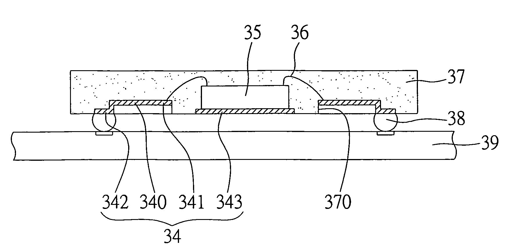
[0034]Referring to FIGS. 3A to 3F, a semiconductor package and a fabrication method thereof according to a first embodiment of the present invention is shown.

[0035]Referring to FIG. 3A, a carrier board 30 made of metal, such as a copper plate, is prepared. The carrier board 30 is covered by a first resist layer 31 having a plurality of first openings 310 for defining extension circuits that subsequently connect with a semiconductor chip.

[0036]Then, an electroplating process is performed to form metal bumps 32 in the first openings 310. The metal bumps 32 can be made of such as copper.

[0037]As shown in FIGS. 3B and 3C, wherein FIG. 3C is a corresponding top view of FIG. 3B, the first resist layer 31 is removed, and the carrier board 30 is covered by a second resist layer 33 having a plurality of second openings 330 that expose the metal bumps 32 and portions of the carrier board 30. As shown in FIG. 3C, the broken lines indicate the metal bumps. The second openings 330 are slightly s...

second embodiment

[0048]Referring to FIG. 4, a semiconductor package and a fabrication method thereof according to a second embodiment is shown.

[0049]The semiconductor package and the fabrication method of this embodiment are similar to those of the first embodiment. The main difference of the present embodiment from the first embodiment is that an insulating layer 48 is filled into the grooves 470 of the encapsulant 47 by such as dispensing so as to protect the extension circuits 440 inside the grooves 470 from exterior damage and contamination.

third embodiment

[0050]Referring to FIG. 5, a bottom view of a semiconductor package and a fabrication method thereof according to a third embodiment of the present invention is shown.

[0051]The semiconductor package and the fabrication method of this embodiment are similar to those of the above embodiments. The main difference is that a guiding groove 59 is formed to connect the grooves 570 on the surface of the encapsulant 57, thereby facilitating filling of an insulating layer 58 in the grooves 570 and the guiding groove 59 by such as dispensing.


PUM


Abstract

A semiconductor package and a fabrication method thereof are disclosed. The fabrication method includes providing a carrier board; forming a plurality of metal bumps on the carrier board; covering on the carrier board a resist layer having openings for exposure of the metal bumps, the openings being smaller than the metal bumps in width such that a metal layer is formed in the openings, the metal layer having extension circuits and extension pads and bonding pads formed on respective ends of the extension circuits; removing the resist layer; electrically connecting at least one semiconductor chip to the bonding pads; forming an encapsulant on the carrier board to encapsulate the semiconductor chip; and removing the carrier board and the metal bumps to expose the metal layer. Therefore, the extension pads of the exposed metal layer can be electrically connected to an external device through a conductive material in subsequent processes, and the extension circuits can be disposed flexibly in accordance with the degree of integration of the chip, so as to reduce the electrical connection path between the chip and the extension circuits.

Description

FIELD OF THE INVENTION[0001]The present invention relates to a semiconductor package and a fabrication method thereof, and more particularly, to a carrier-free semiconductor package and a fabrication method thereof.BACKGROUND OF THE INVENTION[0002]There are various types of semiconductor packages that use lead frames as chip carriers. As for a QFN (Quad Flat Non-leaded) semiconductor package, there is no outer lead as can be found in a traditional QFP (Quad Flat Package) semiconductor package for external electrical connection. As a result, the size of a QFN semiconductor package can be reduced.[0003]However, sometimes, the overall height of the QFN package cannot be further reduced due to thickness of the encapsulant. Thus, in order to meet the need for more compact and lighter semiconductor products, a carrier-free semiconductor package is proposed, which becomes much lighter and thinner by reducing the thickness of the lead frame.[0004]Referring to FIG. 1, a carrier-free semicond...

Claims


Application Information

Patent Timeline
IPC IPC(8): H01L21/50H01L23/00
CPCH01L21/568H01L21/6835H01L24/48H01L24/49H01L24/81H01L24/85H01L24/97H01L2221/68345H01L2224/48091H01L2224/48227H01L2224/48233H01L2224/49109H01L2224/81801H01L2224/85H01L2224/97H01L2924/00014H01L2924/01029H01L2924/01033H01L2924/01046H01L2924/01078H01L2924/01079H01L2924/01082H01L2924/15311H01L2924/181H01L2924/19041H01L2924/19105H01L2924/00H01L2924/00012H01L2224/45015H01L2924/207H01L2224/45099
Inventor LI, YUAN-CHUNHUANG, CHIEN-PINGCHIANG, LIEN-CHENSHYU, WE-HORNGWANG, CHIH-SHIANG
Owner SILICONWARE PRECISION IND CO LTD
Why Eureka
Try Eureka