

Method for Manufacturing Bonded Wafer and Bonded Wafer
- Summary
- Abstract
- Description
- Claims
- Application Information
AI Technical Summary
Benefits of technology
Problems solved by technology
Method used
Image

Examples
example 1
[0095]First, mirror-polished CZ wafers each having a diameter of 200 mm, conductivity type: p-type, and a resistivity of 4 to 6 Ω·cm were prepared. These wafers were used as a base wafer and a bond wafer.
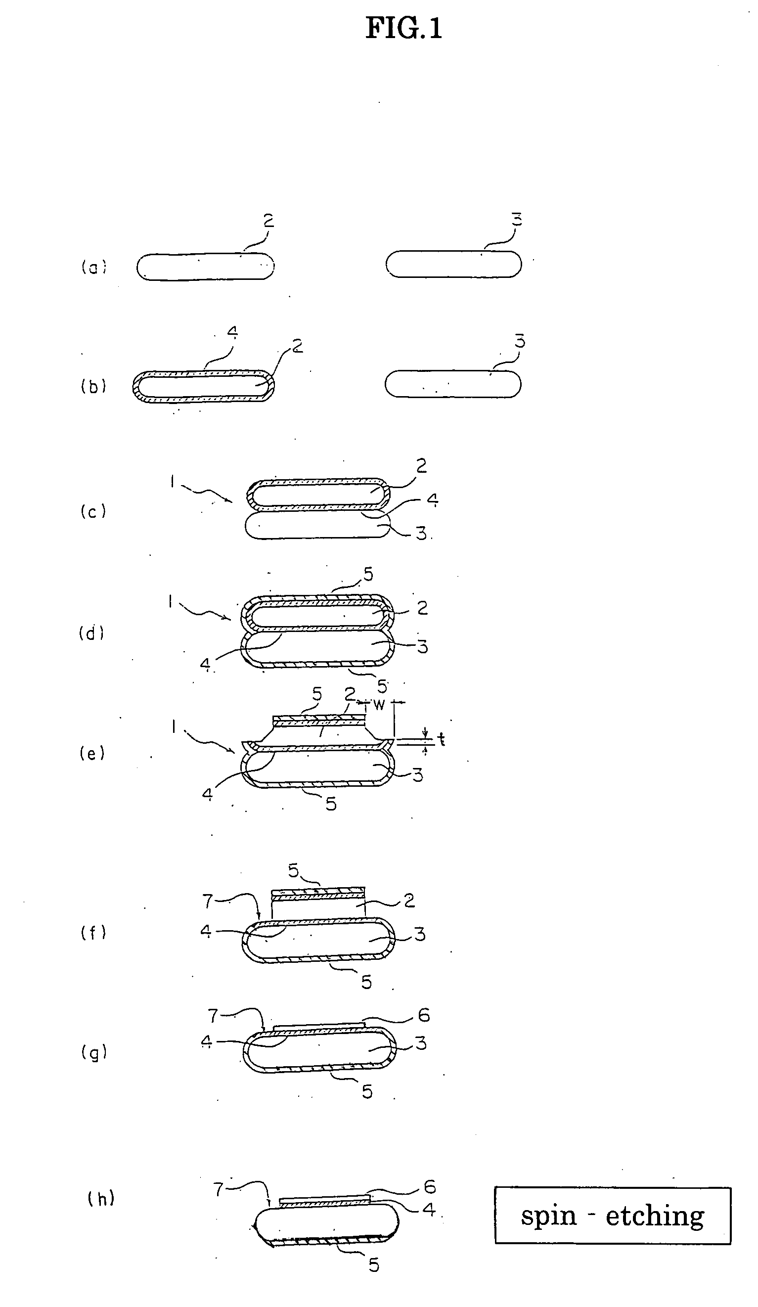
[0096]These wafers were brought into close contact with each other according to the steps (a) to (c) in FIG. 1. Then the wafers were subjected to a bonding heat treatment at 1150° C. under an oxidizing atmosphere for 3 hours to prepare a bonded wafer 1 in FIG. 1(d).
[0097]Next, as shown in FIG. 1(e), the outer periphery of the bond wafer 2 was ground with a grinding machine from the outer periphery toward the center of the wafer. The thickness t was 50 μm.
[0098]Then unbonded portions in the outer periphery of the bond wafer 2 were removed by etching. An etchant used in the etching was NaOH. The whole wafers were immersed, in NaOH to conduct the etching. Etching removal was 90 μm. Thus a wafer shown in FIG. 1(f) was obtained.
[0099]Subsequently, the surface of the bond wafer 2 was thin...
example 2
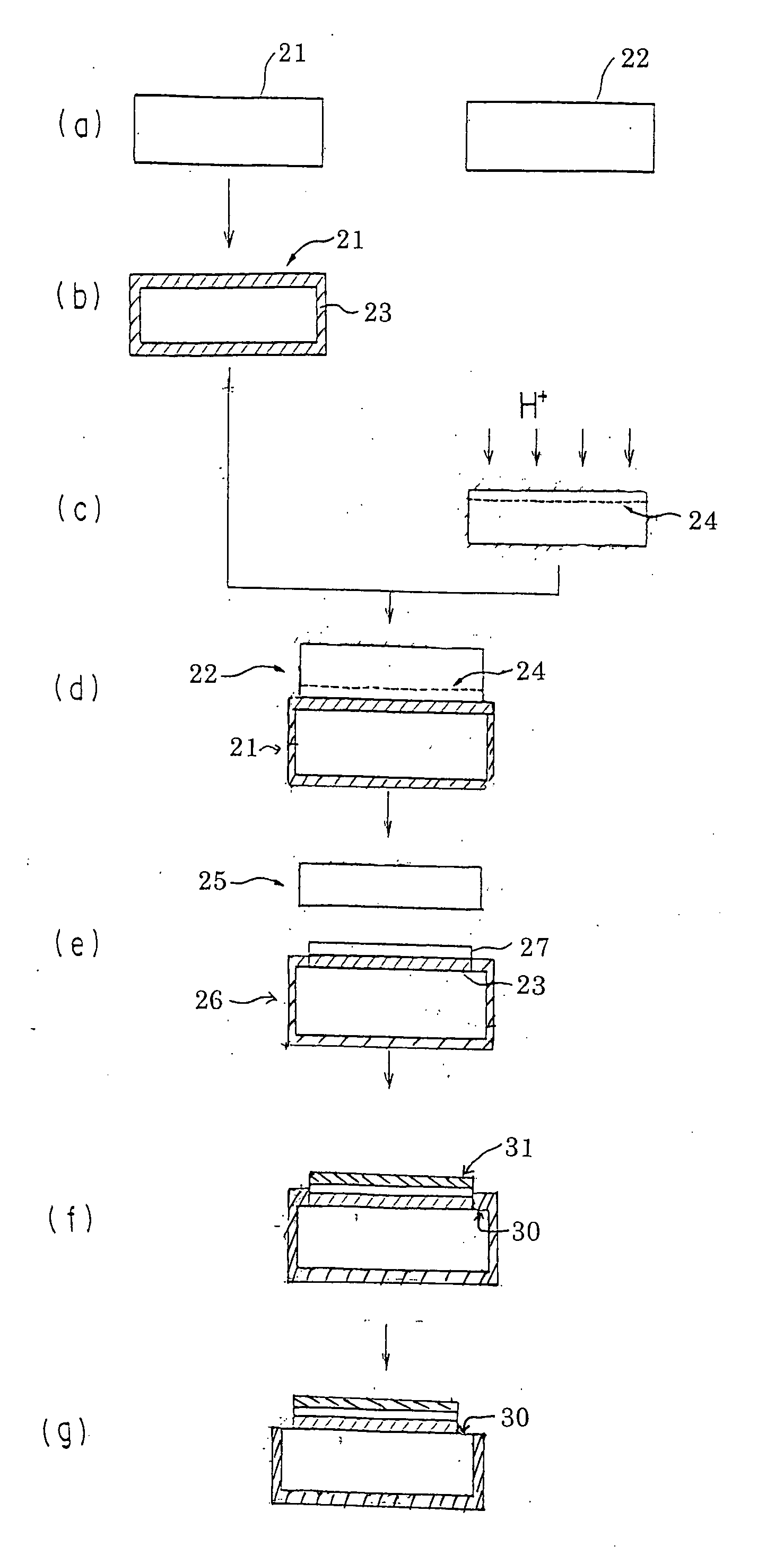
[0103]First, mirror-polished CZ wafers each having a diameter of 200 mm, conductivity type: p-type, and a resistivity of 4 to 6 Ω·-cm were prepared. These wafers were used as a base wafer and a bond wafer. As shown in FIG. 5, a 5 μm thick oxide film was formed on the base wafer, and an Si layer of the bond wafer was transferred to the base wafer by Smart Cut method (registered trademark) to obtain an SOI wafer. After that, a stabilizing heat treatment was conducted.
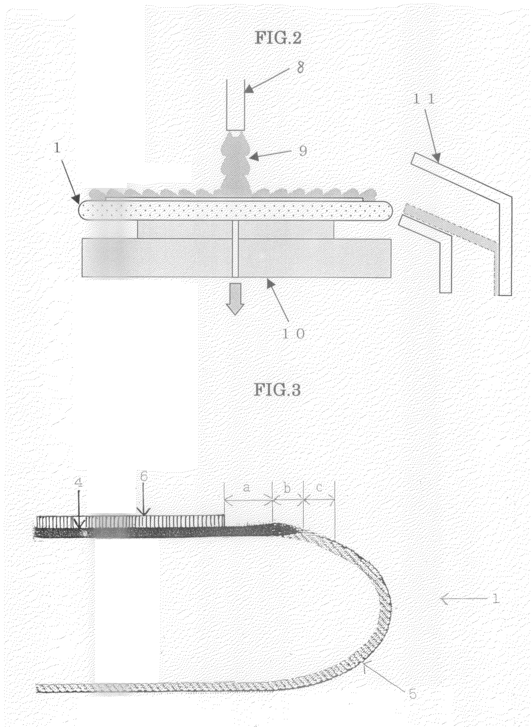
[0104]The SOI wafer has the 5 μm thick oxide film in its terrace region. This oxide film was removed by spin-etching with an apparatus shown in FIG. 6. A 50% aqueous solution of HF was used as an etchant. The etchant was provided directly to the terrace region for 5 minutes to remove the oxide film in the terrace region. During the spin-etching, pure water was provided to the central portion of the SOI wafer as a fluid 12 for protecting the SOI layer from the etchant. After that, the wafer was rinsed for 2 minutes to remo...
example 3
[0107]First, mirror-polished CZ wafers each having a diameter of 200 mm, conductivity type: p-type, and a resistivity of 4 to 6 Ω·cm were prepared. These wafers were used as a base wafer and a bond wafer. As shown in FIG. 5, a 400 nm thick oxide film was formed on the base wafer, a Si layer of the bond wafer was transferred to the base wafer by Smart Cut method (registered trademark) to obtain an SOI wafer. After that, a stabilizing heat treatment was conducted.
[0108]The SOI wafer has the 400 nm thick oxide film in its terrace region. This oxide film was removed by spin-etching with an apparatus shown in FIG. 6. A 50% aqueous solution of HF was used as an etchant. The etchant was provided directly to the terrace region for a minute to remove the oxide film in the terrace region. During the spin-etching, pure water was provided to the central portion of the SOI wafer as a fluid 12 for protecting the SOI layer from the etchant. After that, the wafer was rinsed for 30 seconds to remove...
PUM
 Abstract
Description
Claims
Application Information