Gettering material for encapsulated microdevices and method of manufacture

a technology of encapsulated microdevices and getter films, which is applied in the direction of semiconductor devices, semiconductor/solid-state device details, electrical apparatus, etc., can solve the problems of affecting the functioning of the device, the tendency of the getter film to delaminate, and the delaminate tendency of the getter film, etc., to reduce the fe composition, reduce the cte, and increase the zr composition

Inactive Publication Date: 2009-01-01
INNOVATIVE MICRO TECH
View PDF4 Cites 13 Cited by
  • Summary
  • Abstract
  • Description
  • Claims
  • Application Information

AI Technical Summary

Benefits of technology

[0014]The systems and methods therefore include determining the CTE of the intended substrate, and adjusting the getter alloy until it has a CTE that more closely approximates that of the substrate. For example, a silicon substrate has a measured CTE of about 3 ppm per degree. The getter composition of a ZrVTiFe getter is then adjusted to increase the Zr composition, with its relatively low CTE of 2.9 ppm per degree, and reduce the Fe composition, with its relatively high CTE of 11.6 ppm. Thus, the new alloy has a CTE that more closely matches silicon, and associated problems of delamination, cracking, and flaking of the getter alloy into the microdevice cavity are reduced or avoided. The getter is thereby better able to perform its intended function of absorbing impurity gases and reducing the pressure of the ambient environment in the microdevice cavity.
[0015]The new getter composition may be applied to an indented lid design, as disclosed in the incorporated '435 application. The indented lid design may have indentation features formed therein, which increase the surface area, and therefore the gettering ability of a getter material formed on the indented lid. Because of the details of the shape of the indented lid, matching the CTEs of the getter material with the lid substrate may provide particular benefits of promoting the adhesion of the getter material to the indented substrate.

Problems solved by technology

The debris generated may interfere with the functioning of the device, or of the getter, or both.
The tendency for the getter film to delaminate may be worse when it is deposited over rough or corrugated surfaces.

Method used


Image

  • Gettering material for encapsulated microdevices and method of manufacture
  • Gettering material for encapsulated microdevices and method of manufacture
  • Gettering material for encapsulated microdevices and method of manufacture

Examples


Embodiment Construction

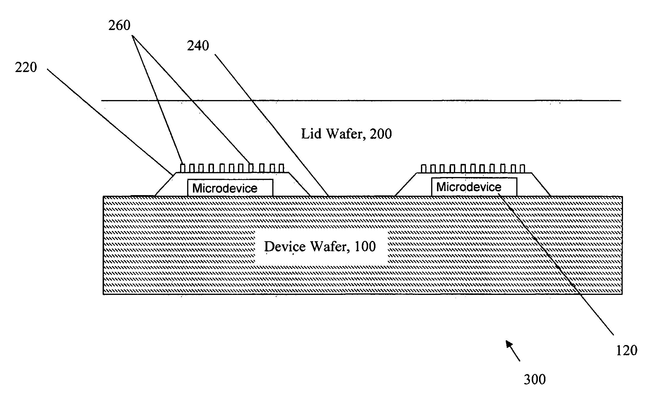
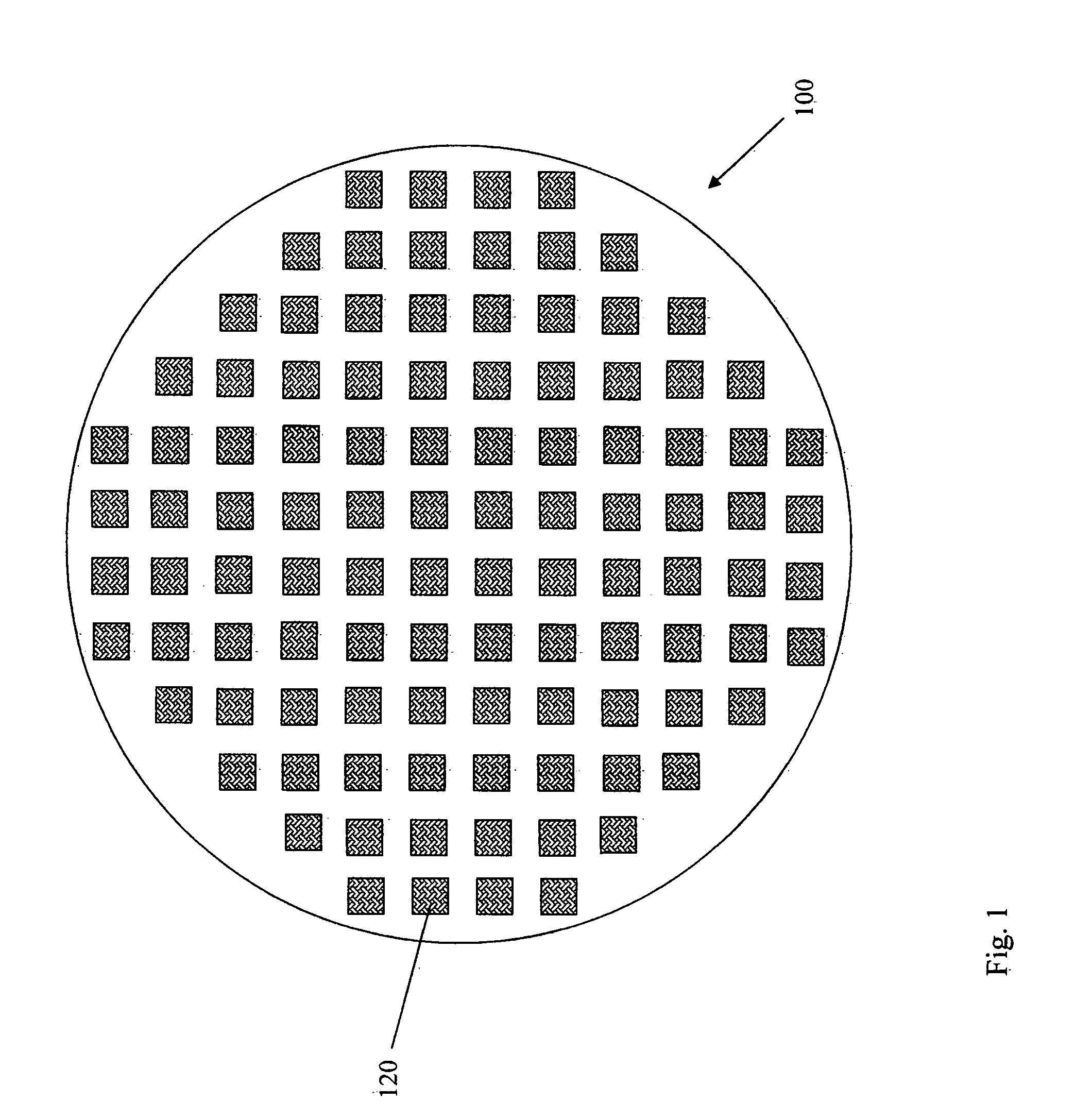
[0026]The systems and methods described herein may be particularly applicable to vacuum encapsulated moveable microelectromechanical (MEMS) devices, such as sensors, actuators, emitters, detectors, switches, cantilevers, or the like. However, they may also be applicable to any integrated circuit formed on a device wafer and encapsulated with a getter material under a lid wafer. Accordingly, the improved getter formulation may be applied to many other types of microdevices, as well as the specific embodiment described below.

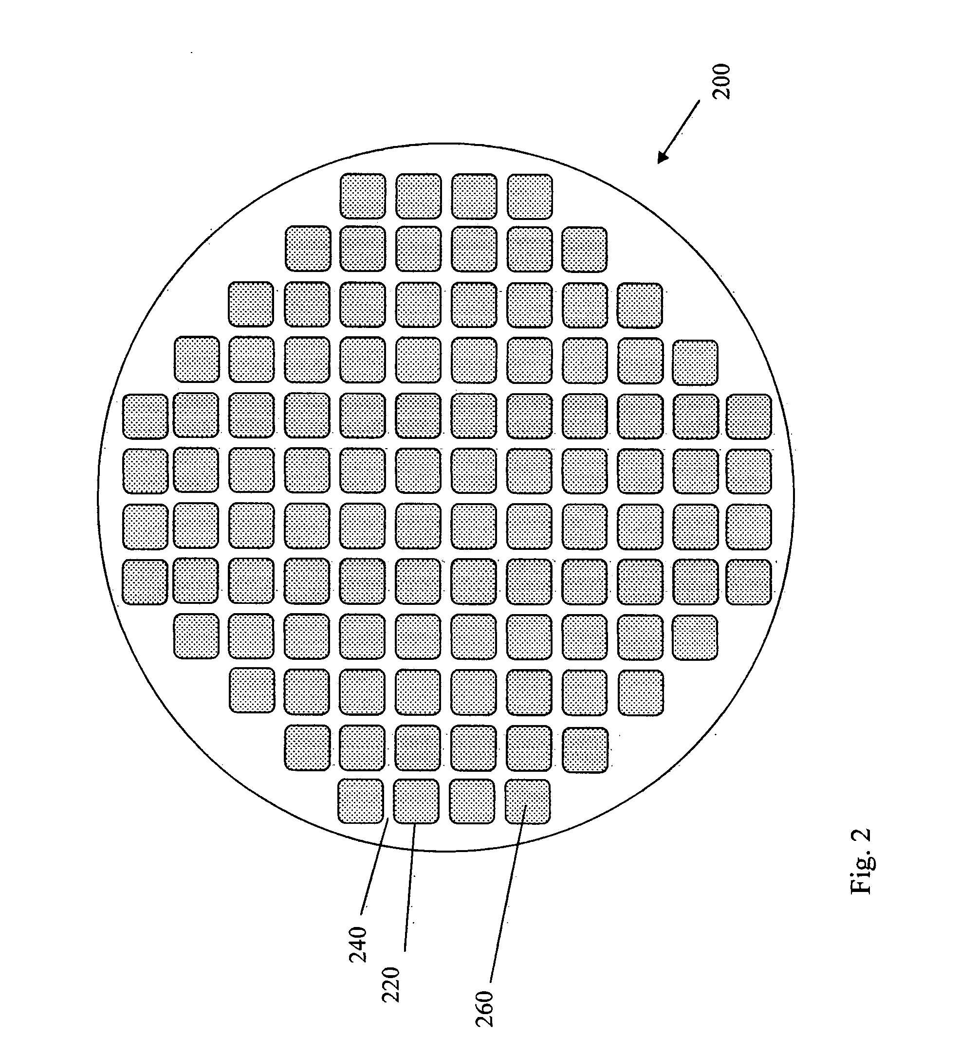
[0027]Furthermore, the systems and methods are described with respect to an indented lid embodiment, wherein the improved getter material is deposited in a cavity having a plurality of indentation features formed therein. However, it should be understood that this embodiment is exemplary only, and that the improved getter material may be applied to other designs, such as an unindented lid. The improved getter material may be applied to a lid or device wafer with n...


PUM

PropertyMeasurementUnit
aspect ratioaaaaaaaaaa
depthaaaaaaaaaa
depthaaaaaaaaaa

Abstract

A method for providing improved gettering in a vacuum encapsulated microdevice is described. The method includes designing a getter alloy to more closely approximate the coefficient of thermal expansion of a substrate upon which the getter alloy is deposited. Such a getter alloy may have a weight percentage of less than about 8% iron (Fe) and greater than about 50% zirconium, with the balance being vanadium and titanium, which may better match the coefficient of thermal expansion of a silicon substrate. In one exemplary embodiment, the improved getter alloy is deposited on a silicon substrate prepared with a plurality of indentation features, which increase the surface area of the substrate exposed to the vacuum. Such a getter alloy is less likely to delaminate from the indented surface of the substrate material during heat-activated steps, such as activating the getter material and bonding a lid wafer to the device wafer supporting the microdevice.

Description

CROSS REFERENCE TO RELATED APPLICATIONS[0001]Not applicable.STATEMENT REGARDING FEDERALLY SPONSORED RESEARCH[0002]Not applicable.STATEMENT REGARDING MICROFICHE APPENDIX[0003]Not applicable.BACKGROUND[0004]This invention relates to encapsulated integrated circuit and microelectromechanical systems (MEMS) devices. More particularly, this invention relates to the prevention, reduction, elimination or purification of outgassing and trapped gases in such devices.[0005]The ability to maintain a low pressure or vacuum for a prolonged period in a microelectronic package is sought after in such diverse areas as display technologies, microelectromechanical systems (MEMS) and high density storage devices. For example, computers, displays, and personal digital assistants may all incorporate devices which utilize electrons to traverse a vacuum gap to excite a phosphor in the case of displays, or to modify a media to create bits in the case of storage devices, for example.[0006]Microelectromechan...

Claims


Application Information

Patent Timeline
Patent Type & Authority Applications(United States)
IPC IPC(8): H01L23/26H01L21/00
CPCB81C1/00285H01L23/10H01L23/26H01L2924/0002H01L2924/00
Inventor SUMMERS, JEFFERY F.
Owner INNOVATIVE MICRO TECH
Why Eureka
Try Eureka