
Copper precursors for thin film deposition

a precursor and copper technology, applied in the field of copper precursors, can solve the problems of limited vertical sidewall coverage of line-of-sight techniques, problems such as the difficulty of tsv vias, and the type of chemistry may present problems

Active Publication Date: 2012-09-11
VERSUM MATERIALS US LLC
View PDF18 Cites 3 Cited by
  • Summary
  • Abstract
  • Description
  • Claims
  • Application Information

AI Technical Summary

Problems solved by technology

However, in certain instances, this type of chemistry may present problems because the released trialkylphosphine ligands may contaminate the reaction chamber and act as undesired N-type silicon dopants.
Currently, physical vapor deposition (PVD) copper is used for this purpose, but this line-of-sight technique is typically limited in its ability to provide vertical sidewall coverage.
This is particularly problematic for TSV vias due to its relatively great depth.
This increased aspect ratio will further compromise the ability of PVD to provide adequately conformal copper seed layers with good sidewall coverage.

Method used


Image

  • Copper precursors for thin film deposition
  • Copper precursors for thin film deposition
  • Copper precursors for thin film deposition

Examples


example 1

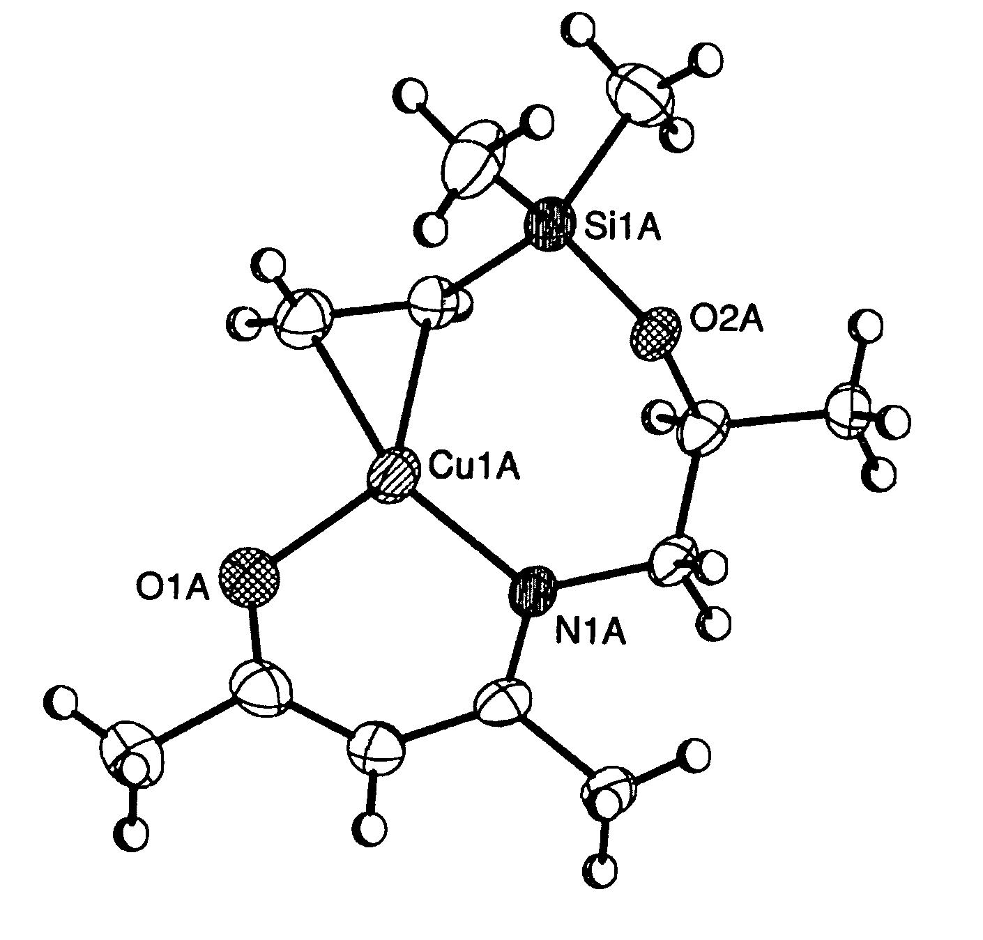
Synthesis of Cu(MeC(O)CHC(NCH2CHMeOSiMe2 C2H3)Me) precursor

Step 1: Forming MeC(O)CHC(HNCH2CHMeOH)Me or Ketoimine Intermediate

[0078]150 g (2.0 moles 1-amino-2-propanol) was added to 200 g (2.0 moles) of 2,4-pentanedione stirred in 1.0 liter of hexane solvent containing 200 g of sodium sulfate drying agent for 1 hour. The hexane was then decanted off and 500 ml of tetrahydrofuran (THF) solvent added to dissolve all of the crude product. This solution was then decanted into a fresh flask containing 200 g of fresh sodium sulfate and stirred for 1 hour. The THF solution was then decanted off and stored in a freezer overnight to crystallize. The supernatant liquid was decanted off and the remaining solid pumped dry. The crude solid was then melted under vacuum to 130 C and volatiles pumped away to a liquid nitrogen cooled vacuum trap. Yield=197.5 g (63%), The GCMS results for the product showed it to be >99% pure and its mass spectra identified as that of the desired product showing a par...

example 2

CVD Deposition of a Copper Film Using the Cu(MeC(O)CHC(NCH2CHMeOSiMe2 C2H3)Me) Precursor

[0081]A copper film was deposited onto a titanium nitride (TiN) substrate using the Cu(MeC(O)CHC(NCH2CHMeOSiMe2 C2H3)Me) precursor in a hot wall CVD laboratory scale reactor using the conditions described in the following Table I and using formic acid as a reducing agent. A pure copper film of approximately 5 microns thick was grown, as determined by Secondary Ion Mass Spectrometry (SIMS) analysis, as shown in FIG. 6, which showed no detectable amounts of carbon, hydrogen, nitrogen, oxygen or silicon meaning that the copper film is >99.99 atomic % pure copper. Note that the depth profile was stopped before the bottom of the copper film was reached.

[0082]

TABLE ICVD copper process conditionsTiN wafer temperature ° C.250Copper Precursor source temperature120(° C.)CVD chamber pressure (Torr)2Copper precursor helium carrier gas flow25(sccm)Formic acid reagent flow (sccm)150Run time (minutes)30

example 3

CVD Deposition of a Copper Film Using the Cu(MeC(O)CHC(NCH2CHMeOSiMe2 C2H3)Me) Precursor

[0083]A copper film was deposited onto a patterned tantalum nitride (TaN) substrate using the Cu(MeC(O)CHC(NCH2CHMeOSiMe2 C2H3)Me) precursor in a hot wall CVD laboratory scale reactor using the conditions described in the following Table II and using formic acid as a reducing agent. The copper film was deposited as a conformal layer into a large scale trench feature and had dimensions typically found in TSV / 3-D packaging, as evidenced by FIGS. 7, 8, 9 and 10 which provide four Scanning Electron Microscope (SEM) images of the trench, top, bottom, and sidewall views, respectively, of the copper film.

[0084]

TABLE IICVD copper process conditionsTaN wafer temperature (° C.)225Copper Precursor source temperature120(° C.)CVD chamber pressure (Torr)5Copper precursor helium carrier gas flow100(sccm)Formic acid reagent flow (sccm)150Run time (minutes)60


PUM

PropertyMeasurementUnit
thicknessaaaaaaaaaa
temperatureaaaaaaaaaa
temperaturesaaaaaaaaaa

Abstract

Non-fluorinated copper precursors and methods for making and using same are described herein. In certain embodiments, the copper precursors described herein may be used as precursors to deposit copper films and alloys thereof on a substrate through, for example, atomic layer deposition or chemical vapor deposition conditions.

Description

CROSS-REFERENCE TO RELATED APPLICATIONS[0001]This application claims the benefit of U.S. Provisional Application No. 60 / 985,428, filed Nov. 5, 2007. The disclosure of this provisional application is incorporated herein by reference in its entirety.BACKGROUND OF THE INVENTION[0002]The present invention generally relates to copper precursors that are used to deposit thin copper films. More specifically, the present invention relates to non-fluorinated copper precursors which are volatile, thermally stable and can be used, for example, to deposit thin copper films using atomic layer deposition (ALD) or chemical vapor deposition (CVD) processes.[0003]The semiconductor industry uses metal-containing interconnects, such as copper (Cu), in electronic devices such as, for example, state of the art microprocessors. The metal-containing interconnects, which may be embedded fine metal lines, form the three dimensional grid upon which millions of transistors at the heart of the microprocessor c...

Claims


Application Information

Patent Timeline
Patent Type & Authority Patents(United States)
IPC IPC(8): C07F7/10H01L29/12C23C16/00C07F1/08
CPCC07F7/1844C23C16/18H01L21/28556H01L21/28562C07F7/1804C07F1/08
Inventor NORMAN, JOHN ANTHONY THOMASPEREZ, MELANIE K.
Owner VERSUM MATERIALS US LLC
Learn More