

High-Resolution, Nondestructive Imaging of Dielectric Materials
a dielectric material, high-resolution technology, applied in the direction of dielectric property measurement, using reradiation, instruments, etc., can solve the problems of cord deterioration, prone to catastrophic failure, and defect can begin, so as to enhance the detection and location of defects, enhance the localization or imaging of features or irregularities, and improve the effect of slop
- Summary
- Abstract
- Description
- Claims
- Application Information
AI Technical Summary
Benefits of technology
Problems solved by technology
Method used
Image

Examples
Embodiment Construction
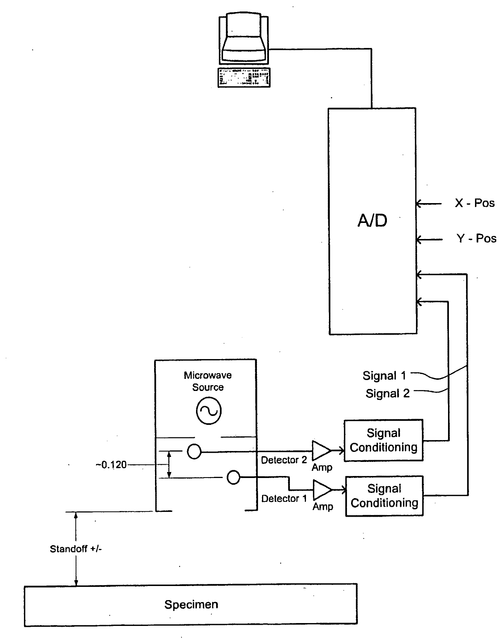
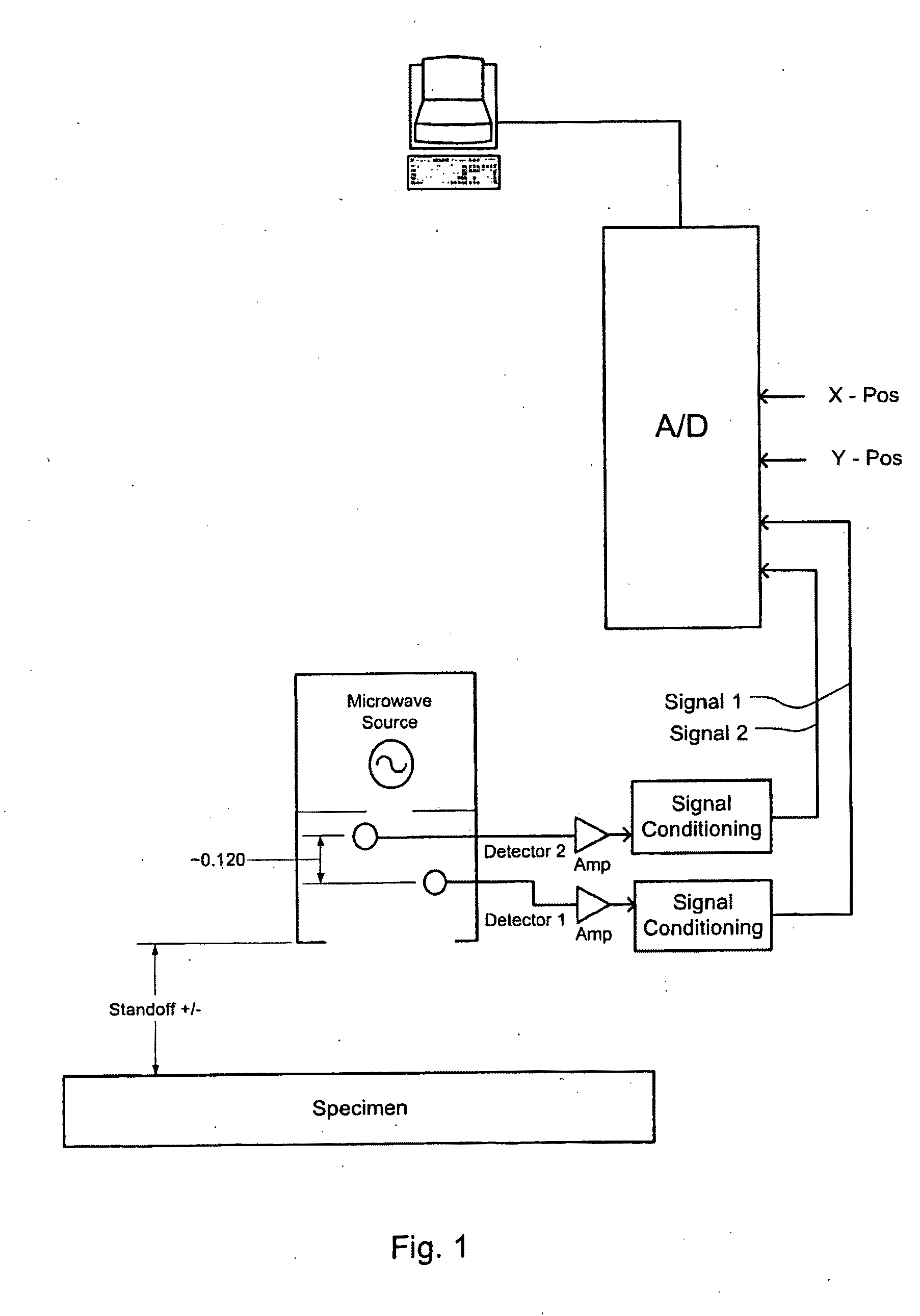
[0039]Substances such as fiberglass that produce noisy reflection patterns in prior ultrasonic techniques may be inspected at low noise levels with the novel microwave technique. For example, the novel technique readily detects many common defects in fiberglass.
[0040]There are many potential fields of use for the invention. As one illustration, the invention may be used to inspect fiber-reinforced plastic (FRP) pipe. Commercially available FRP pipe is a complex composite structure, typically containing many layers of varying composition, density, and dielectric constant. When microwaves are directed towards an FRP pipe, reflections return from all interfaces between materials of different dielectric constant. The returning signal is thus a superposition of many different waveforms, essentially identical in frequency, but generally differing in phase and amplitude. In general, the full thickness of the material is inspected, and all interfaces upon which the microwaves impinge contri...
PUM
| Property | Measurement | Unit |
|---|---|---|
| thick | aaaaa | aaaaa |
| thick | aaaaa | aaaaa |
| thick | aaaaa | aaaaa |
Abstract
Description
Claims
Application Information