
Enhanced Reliability of Wafer-Level Chip-Scale Packaging (WLCSP) Die Separation Using Dry Etching

Active Publication Date: 2009-01-08
TAIWAN SEMICON MFG CO LTD
View PDF48 Cites 97 Cited by
  • Summary
  • Abstract
  • Description
  • Claims
  • Application Information

AI Technical Summary

Benefits of technology

[0013]In accordance with another preferred embodiment of the present invention, a method for enhancing a reliability of wafer-level chip-scale packaging (WLCSP) includes creating a plurality of wafer-level contacts on a front-side surface of a semiconductor wafer. A plurality of grooves is dry etched onto the front-side surface, where the grooves define one or more boundaries between each of a plurality of die within the semiconductor wafer. The front-side surface is then sealed with an encapsulating material. A die saw saws through the encapsulating material at the grooves, where the sawing leaves a piece of substrate material on the backside of the semiconductor wafer. Each of the plurality of die is separated by polishing the backside to remove the piece of substrate material.
[0014]An advantage of a preferred embodiment of the present invention is that by using dry etching, which is typically more expensive that the commonly-used wet etching techniques, smoother sidewalls result in the grooves. The smoother surface lowers the risk of cracking or splaying than the risk present in the rougher-edged walls created by wet etching, dicing, or laser grooving.
[0015]A further advantage of a preferred embodiment of the present invention is that the quality of the separated die is improved by sawing the recesses into the wafer before the backside grinding or polishing separates the individual die. When the die are separated or singulated directly from a sawing / dicing process, the chances of cracking or splaying are increased, especially with narrow dicing streets of 60 μm or less.

Problems solved by technology

However, increased pin count peripherally designed and arranged around the package typically results in too short of a pitch of lead wire, yielding limitations in board mounting of the packaged chip.
One disadvantage of the prior art is that the wafer may sometimes crack or splay at the die edge, thus, diminishing the integrity and reliability of the integrated circuit (IC) chip.
Faulty die diminish the return on investment to the semiconductor manufacturers and, thus, raises the costs for each individual IC die.
However, while the laser-cut die saw groove lowers the chance of splaying or cracking, such damage continues to be an occurrence.
However, damage continues because the wafer saws still operate to separate or singulate the die from the wafer.

Method used


Image

  • Enhanced Reliability of Wafer-Level Chip-Scale Packaging (WLCSP) Die Separation Using Dry Etching
  • Enhanced Reliability of Wafer-Level Chip-Scale Packaging (WLCSP) Die Separation Using Dry Etching
  • Enhanced Reliability of Wafer-Level Chip-Scale Packaging (WLCSP) Die Separation Using Dry Etching

Examples


Embodiment Construction

[0024]The making and using of the presently preferred embodiments are discussed in detail below. It should be appreciated, however, that the present invention provides many applicable inventive concepts that can be embodied in a wide variety of specific contexts. The specific embodiments discussed are merely illustrative of specific ways to make and use the invention, and do not limit the scope of the invention.

[0025]The present invention will be described with respect to preferred embodiments in a specific context, namely a silicon wafer implementing WLCSP using copper posts. The invention may also be applied, however, to other wafer and process materials.

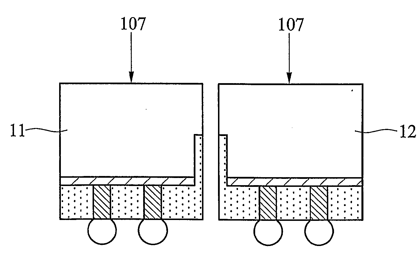
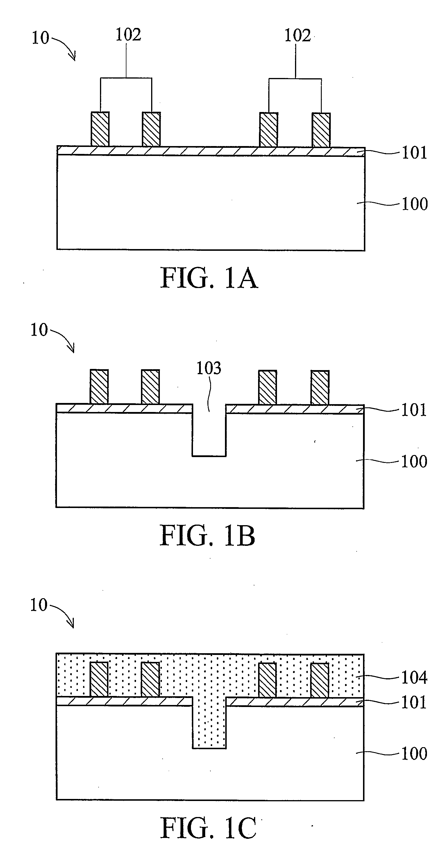
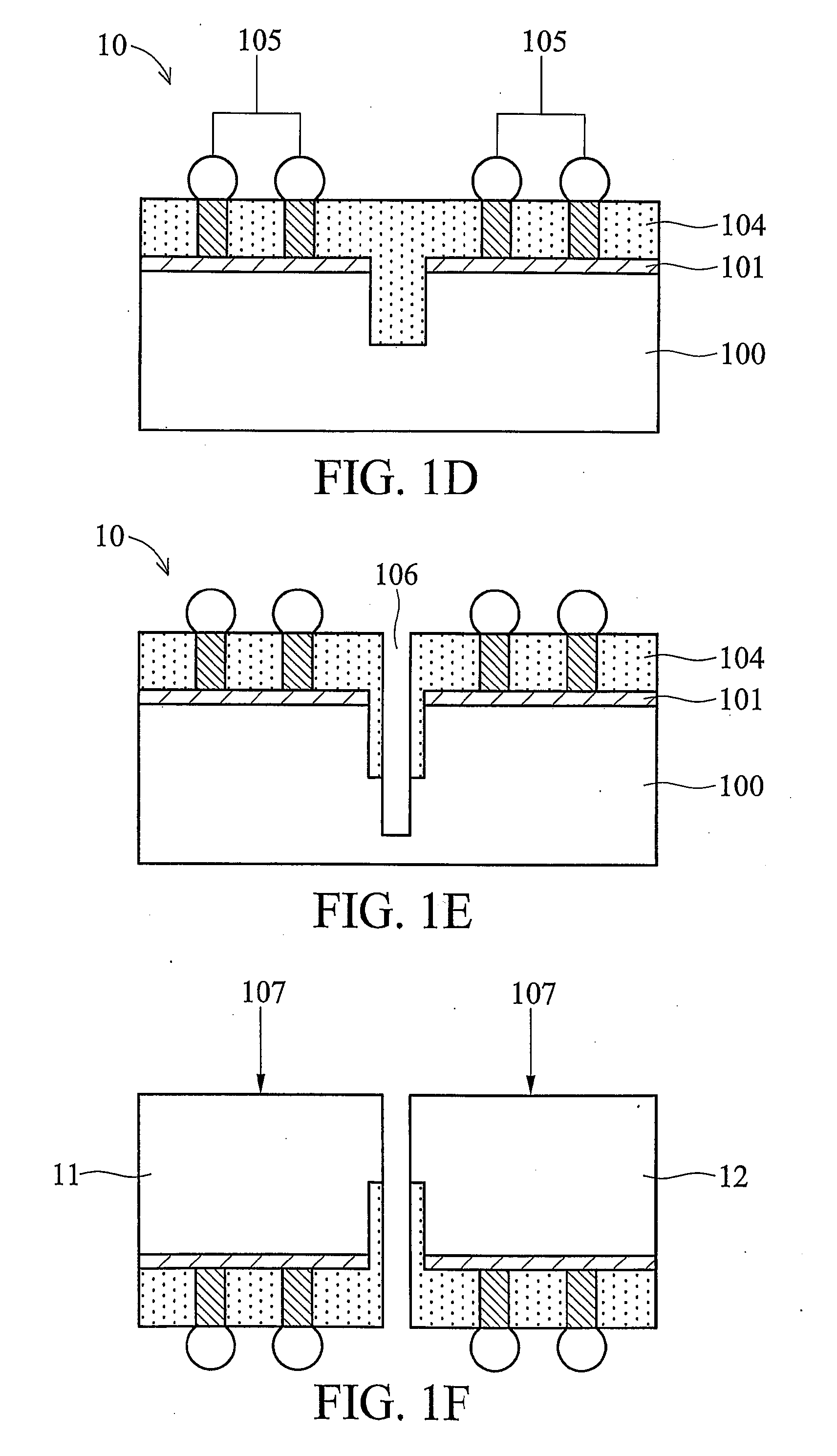
[0026]With reference now to FIG. 1A, there is shown a cross-sectional view of wafer portion 10 at an early stage in implementing a WLCSP process according to one embodiment of the present invention. Wafer portion 10 is only a small part of a larger wafer used in fabricating semiconductor IC devices. Wafer portion 10 includes silic...


PUM


Abstract

An improved Wafer-Level Chip-Scale Packaging (WLCSP) process is described that includes forming a plurality of conductive pillars on a first surface of a semiconductor wafer. One or more grooves are dry etched into the first surface of the semiconductor wafer, where the grooves define at least one boundary between each of a plurality of die within the semiconductor wafer. A layer of encapsulating material is deposited over the first surface. A recess is then cut in each of the grooves through the encapsulating material, where the cutting leaves a piece of semiconductor material on the second surface of the semiconductor wafer. The second surface is then ground to remove the piece of semiconductor material, where the removal of this material separates the plurality of die.

Description

TECHNICAL FIELD[0001]The present invention relates generally to wafer level chip scale packaging (WLCSP), and more particularly to enhancing the reliability of die separation in WLCSP wafers through dry etching.BACKGROUND[0002]The past few decades have seen many shifts in electronics and semiconductor packaging that have impacted the entire semiconductor industry. The introduction of surface-mount technology (SMT), such as ball grid array (BGA), land grid array (LGA), and similar types of packages, were generally important steps for high-throughput assembly of a wide variety of integrated circuit (IC) devices, while, at the same time, allowing reduction of the pad pitch on the printed circuit board. Conventionally packaged ICs have a structure basically interconnected by fine gold wire between metal pads on the die and electrodes spreading out of molded resin packages. Dual Inline Package (DIP) and Quad Flat Package (QFP) are fundamental structures of current IC packaging. However, ...

Claims


Application Information

Patent Timeline
IPC IPC(8): H01L21/00
CPCH01L21/561H01L23/3114H01L23/3178H01L23/3185H01L24/03H01L24/05H01L2224/13023H01L24/13H01L2224/16H01L2924/01078H01L2924/01079H01L2924/10157H01L2924/14H01L24/11H01L2224/0401H01L2224/94H01L2224/03H01L2224/11
Inventor KARTA, TJANDRA WINATAHSU, STEVENLEE, CHIEN-HSIUNWU, GENELIANG, JIMMY
Owner TAIWAN SEMICON MFG CO LTD
Learn More