Semiconductor Device and Method for Manufacturing Same

Active Publication Date: 2009-01-22
ROHM CO LTD
View PDF6 Cites 5 Cited by
  • Summary
  • Abstract
  • Description
  • Claims
  • Application Information

AI Technical Summary

Benefits of technology

[0012]It is therefore the first objective of the present invention to provide a semiconductor device that has a structure that uses SiC semiconductor and provides stable device properties and a method of manufactur

Problems solved by technology

As a matter of course, in this case, reproducibility cannot be expected from the displacement of the m

Method used


Image

  • Semiconductor Device and Method for Manufacturing Same
  • Semiconductor Device and Method for Manufacturing Same
  • Semiconductor Device and Method for Manufacturing Same

Examples


Embodiment Construction

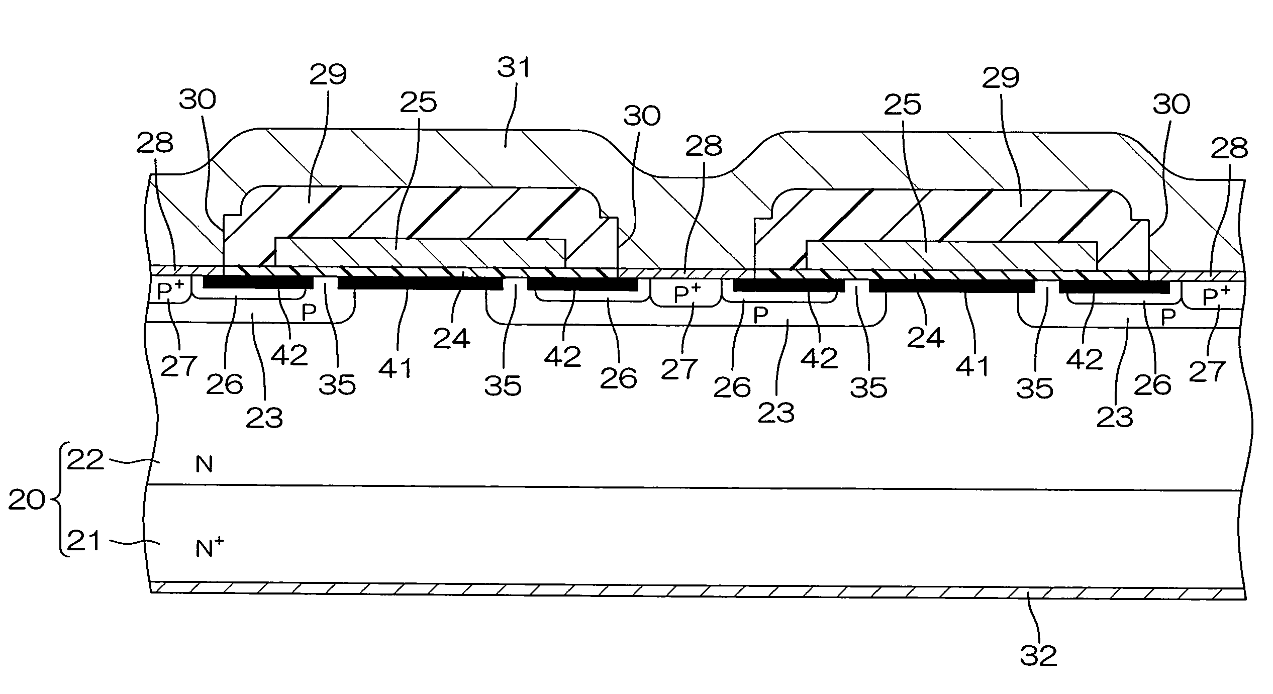
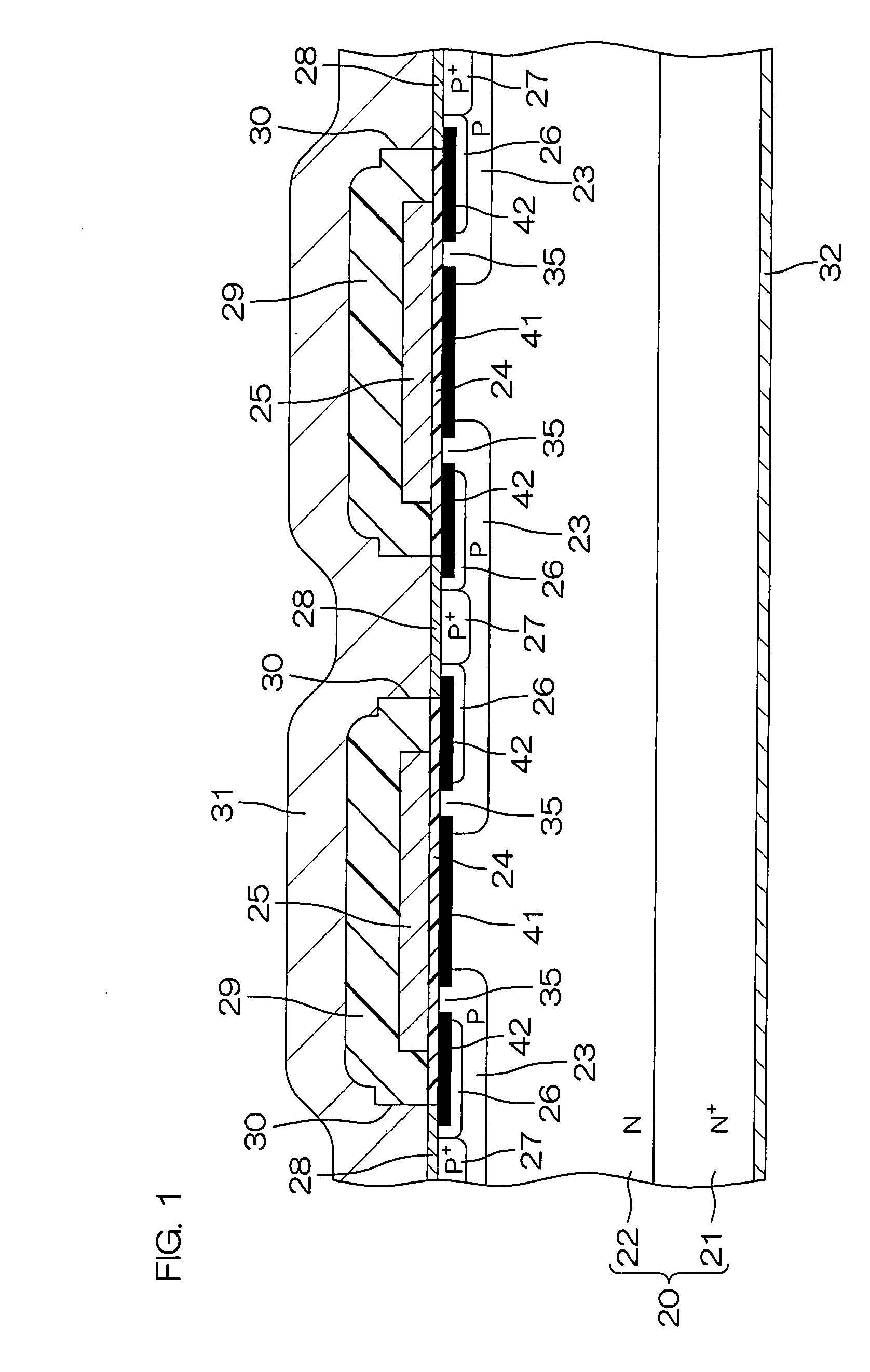
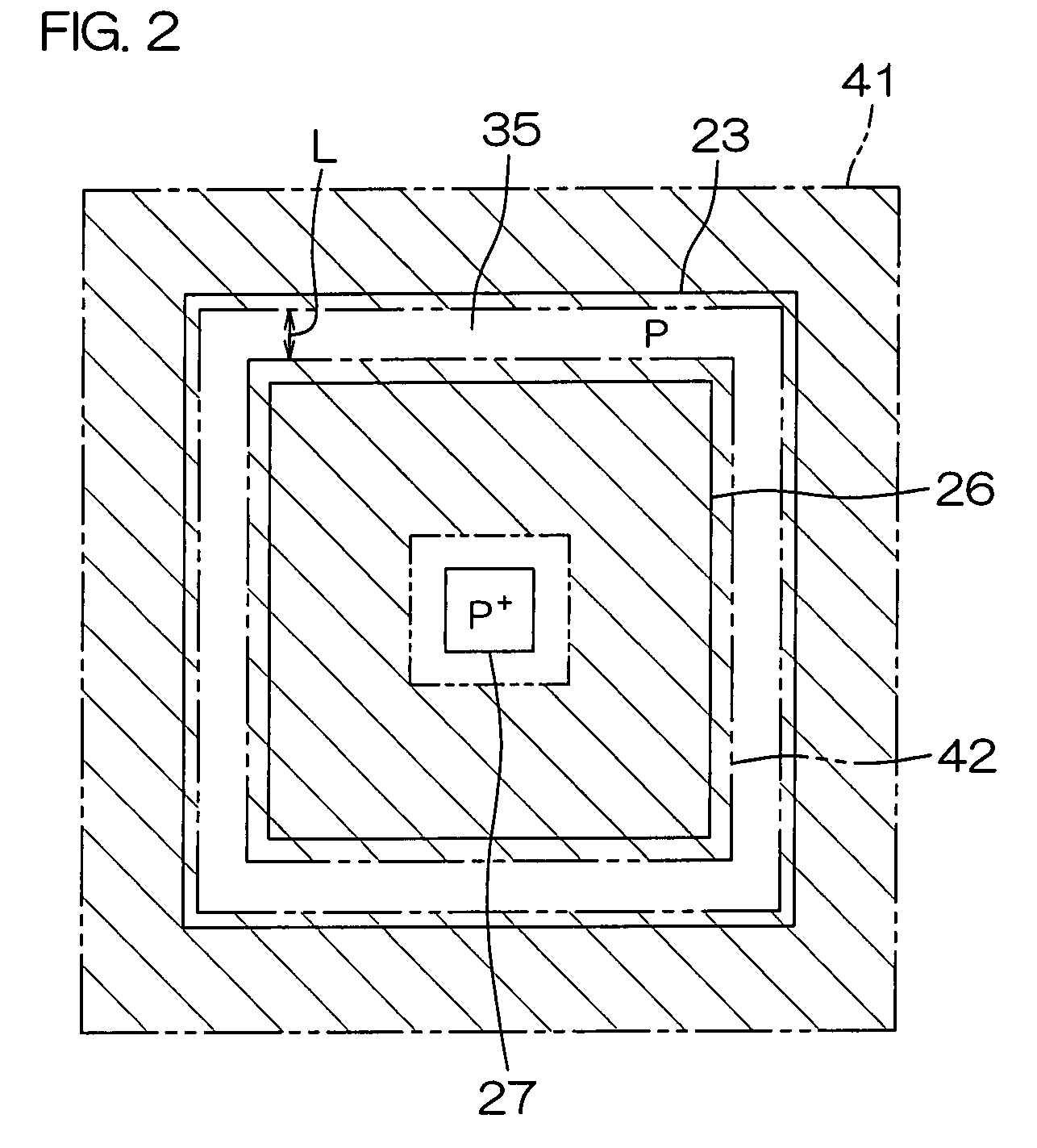
[0031]FIG. 1 is a schematic sectional view for describing an arrangement of a power MOSFET as an individual semiconductor element according to a first embodiment of the present invention. The power MOSFET comprises a SiC semiconductor substrate 20 that is formed by growing a N type SiC epitaxial layer 22 on a N+ type SiC substrate 21. A plurality of P type wells 23 are formed in spaced relation on the surface portion of an N type epitaxial layer 22. In this embodiment, each of the P type wells 23 is formed in, for example, a rectangular shape (including a square), and the rectangular shaped P type wells 23 are distributed, for example, in grid on the SiC semiconductor substrate 20, as shown in a schematic plan view of FIG. 2.

[0032]On the surface of the SiC semiconductor substrate 20, gate electrodes 25 are formed so as to spread across the region of the adjacent P type wells 23 with gate insulating films 24 sandwitched between the SiC semiconductor substrate 20 and the gate electrod...


PUM


Abstract

A semiconductor device includes a first conductive type SiC semiconductor substrate; a second conductive type well formed on the SiC semiconductor substrate; a first impurity diffusion layer formed by introducing a first conductive type impurity so as to be partly overlapped with the well in a region surrounding the well; a second impurity diffusion layer formed by introducing the first conductive type impurity in a region spaced apart for a predetermined distance from the impurity diffusion layer in the well; and a gate electrode opposed to a channel region between the first and the second impurity diffusion layers with gate insulating film sandwiched therebetween.

Description

TECHNICAL FIELD[0001]The present invention relates to a semiconductor device using a SiC (silicon carbide) semiconductor substrate and a method of manufacturing the same.DESCRIPTION OF THE RELATED ART [0002]Conventionally, a power MOSFET using Si (silicon) semiconductor substrate has been used for a power source (particularly those using an inverter) in household consumer electric appliances and electric vehicles (hybrid electric vehicles, for example).In the field of power electronics, power loss in the devices during power conversion has been a problem and attempts have been made to reduce the loss. It has been said, however, the Power MOSFET formed of Si materials have almost achieved its technical limitations and it has come to a difficult phase to further pursue higher efficiency.[0003]With this technical background, there has been a study on the application of SiC semiconductors to power devices. SiC is a compound with excellent physical properties. For example, SiC has about ...

Claims


Application Information

Patent Timeline
IPC IPC(8): H01L21/336H01L29/24
CPCH01L29/0696H01L29/086H01L29/7802H01L29/1608H01L29/66068H01L29/0878
Inventor MIURA, MINEO
Owner ROHM CO LTD
Why Eureka
Try Eureka