

Organic EL Display Device
a display device and organic el technology, applied in the direction of discharge tube/lamp details, organic semiconductor devices, lamp incadescent bodies, etc., can solve the problems of low accuracy of vapor deposition, inability to realize high brightness, and high melting point of conventional auxiliary electrodes, so as to prolong the life of organic el display devices. the effect of low manufacturing temperature and prolonged life of organic el elements
- Summary
- Abstract
- Description
- Claims
- Application Information
AI Technical Summary
Benefits of technology
Problems solved by technology
Method used
Image

Examples
embodiment 1
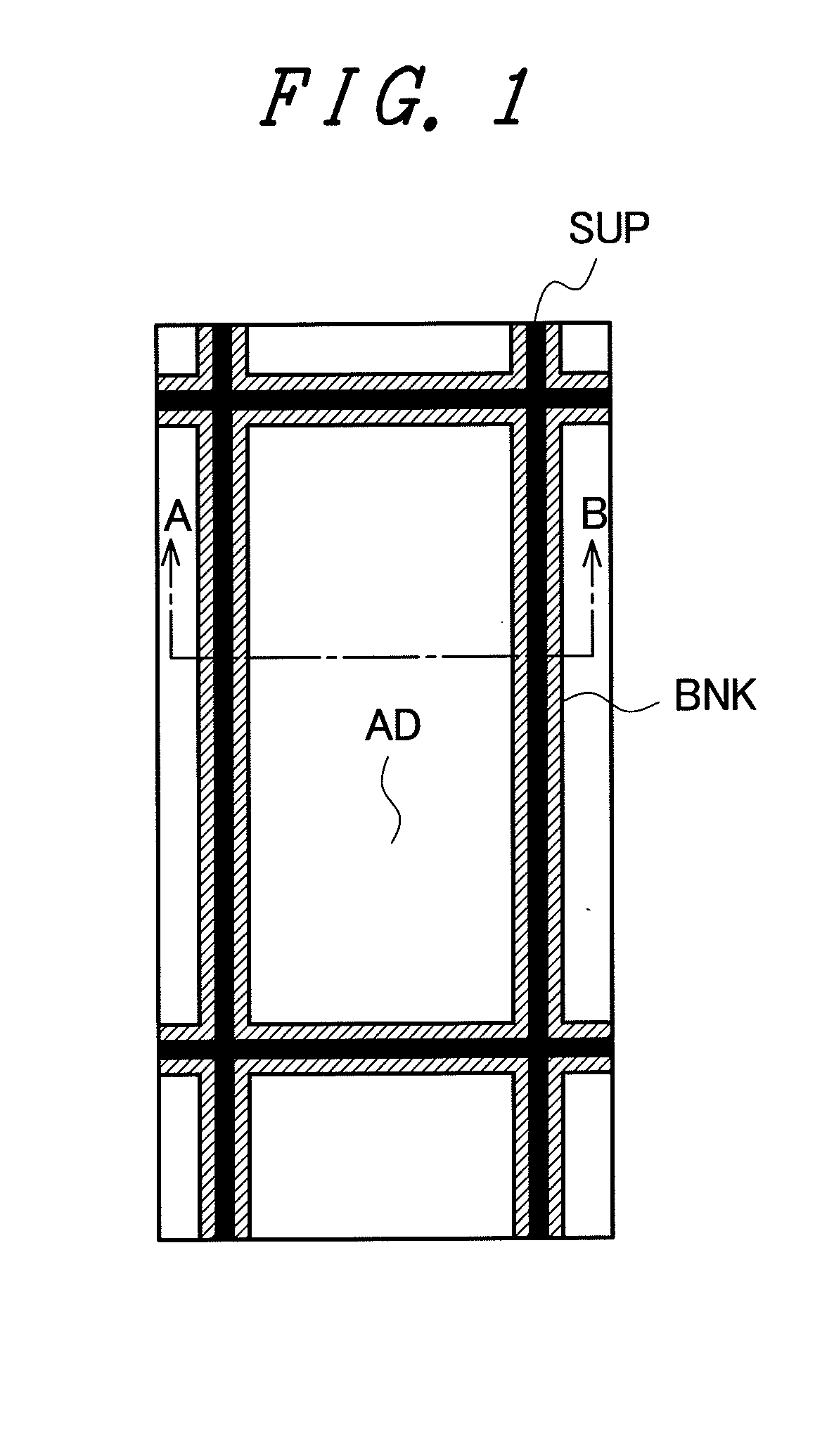
[0026]An organic EL display device of the present invention includes an EL substrate on which organic EL elements are formed and a sealing substrate which covers the organic EL elements. FIG. 1 is a partial top plan view of an effective display region of the EL substrate to which the present invention is applied. Anodes constituting pixel electrodes AD are arranged in a matrix array with a predetermined distance therebetween. Further, a pixel separation film BNK is formed in a grid pattern so as to expose the centers of respective pixel electrodes AD. An auxiliary electrode SUP is arranged at positions where the auxiliary electrode SUP and the pixel separation film BNK overlap with each other. Further, a cathode which constitutes a common electrode CD is formed on the whole display region below the auxiliary electrode SUP.
(Layer Structure)
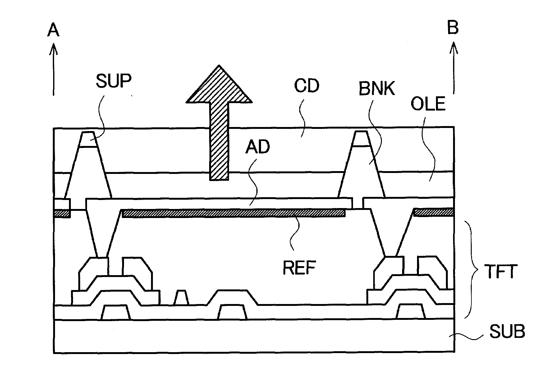
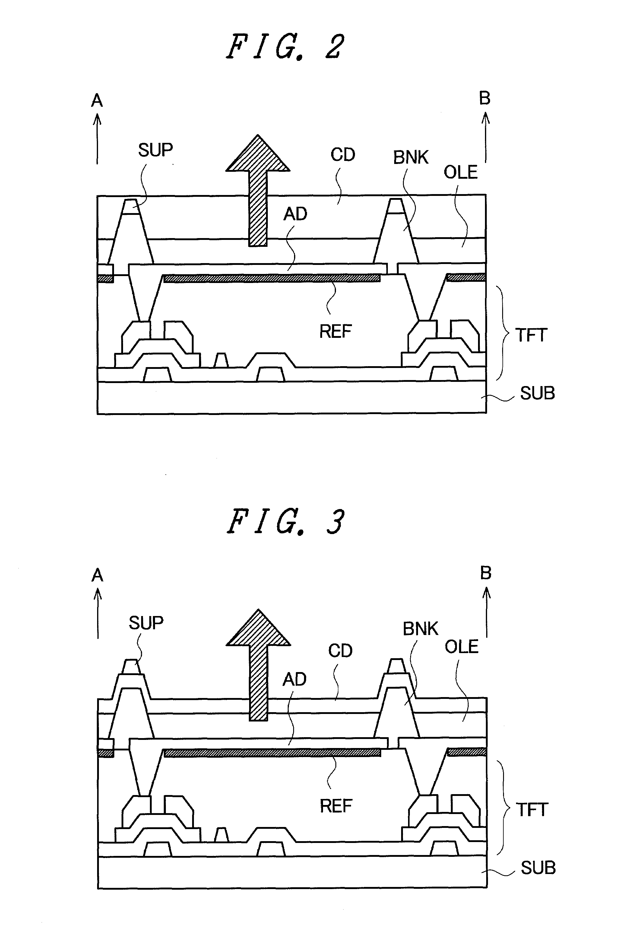
[0027]FIG. 2 is a cross-sectional view taken along a line A-B in FIG. 1. In FIG. 2, on a circuit layer including thin film transistors TFT, reflec...
embodiment 2
[0030]FIG. 1 is a partial top plan view of an effective display region of the organic EL display device to which the present invention is applied.
[0031]FIG. 3 is a partial cross-sectional view of the effective display region of the organic EL display device to which the present invention is applied.
(Layer Structure)
[0032]FIG. 3 is a cross-sectional view taken along a line A-B in FIG. 1. In FIG. 3, on a circuit layer including thin film transistors TFT, reflection films REF, pixel electrodes AD, a pixel separation film BNK, an organic EL layer OLE, a common electrode CD, and an auxiliary electrode SUP are sequentially stacked in this order. A channel of the thin film transistor TFT is formed of a semiconductor layer made of amorphous silicon to which crystallinity is imparted, wherein the reflection film REF is formed of a stacked film made of AlSi / MoW, the pixel electrode AD is made of ITO, the pixel separation film BNK is made of polyimide or SiN, the common electrode CD is made of...
PUM
 Abstract
Description
Claims
Application Information