Photosensor

a photosensor and flat panel technology, applied in the field of flat panel photosensors, can solve the problems of low spatial resolution of the pickup tube, low sensitivity, and inadequacies of instantaneous us

Inactive Publication Date: 2009-01-29
MITSUBISHI ELECTRIC CORP
View PDF10 Cites 57 Cited by
  • Summary
  • Abstract
  • Description
  • Claims
  • Application Information

AI Technical Summary

Benefits of technology

[0011]A margin for an opening size for connection between a source electrode and a gate electrode need not be considered, and a step difference formed by a contact hole is eliminated in a formation area for Si layers, which constitute a photodiode provided for a photosensor. Thus, an uneven growth of an Si layer at the step difference can be prevented, and the occurrence of a membrane stress at the step difference can be prevented. As a result, a homogeneous Si layer is obtained for a photodiode, and a leak current of a photosensor can be inhibited.

Problems solved by technology

The X-ray film provides a high spatial resolution, but there are several drawbacks: the X-ray film has a low sensitivity and enables radiographing of only still pictures, and since the developing process is required after radiographing, this is not appropriate for instantaneous use.
However, the image pickup tube has a low spatial resolution, and since this is a vacuum device, the increase of the device size is limited.
Accordingly, surface roughness occurs and a leak current from the photodiode is increased.
In this case, an aluminum alloy film having a low resistance can not be employed to form a gate electrode and gate wiring.
However, in this structure, it is found through our evaluation that, when the opening edge length obtained by adding the lengths of edges, i.e., the circumferential length of the opening of the contact hole was increased, the current leak element was increased.

Method used


Image

  • Photosensor
  • Photosensor
  • Photosensor

Examples


first embodiment

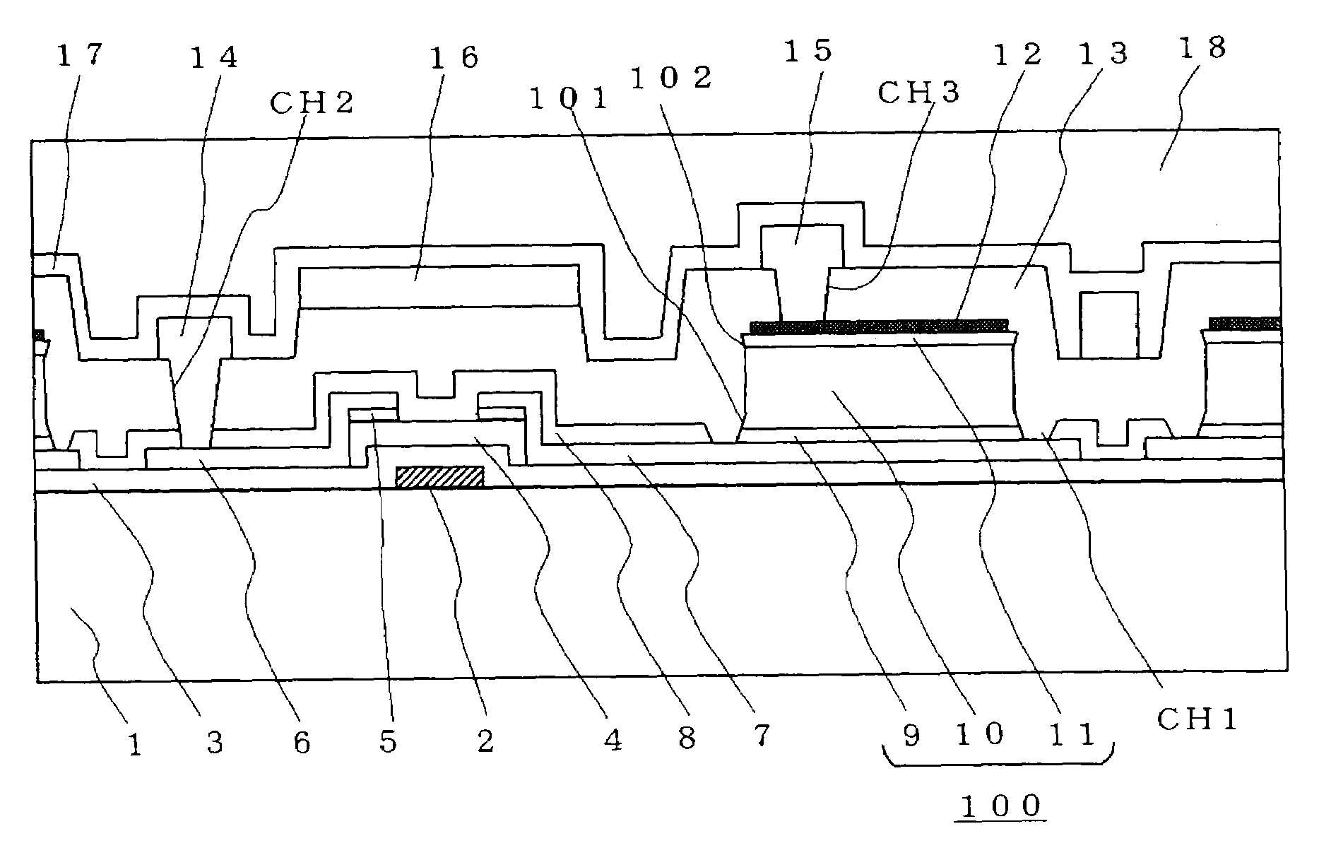
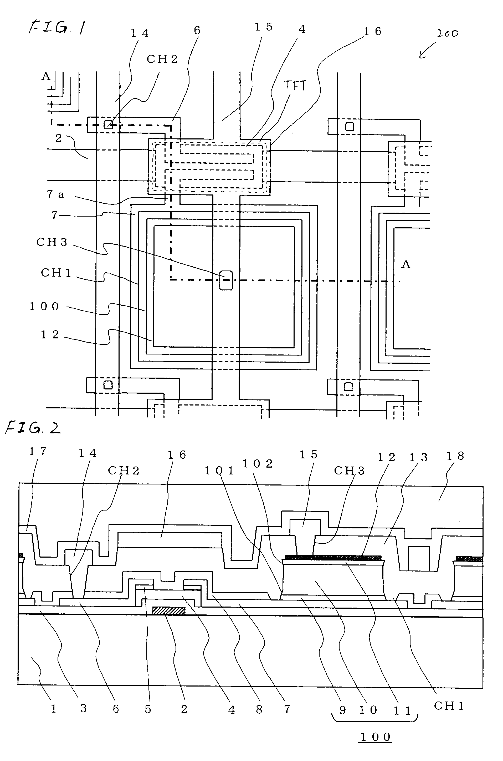
[0032]The preferred embodiments of the present invention will be specifically described while referring to drawings. FIG. 1 is a plan view of a TFT array substrate 200 provided for a photosensor according to a first embodiment of this invention. FIG. 2 is a cross-sectional view of a portion indicated by A-A in FIG. 1.

[0033]A gate electrode 2 is made of metal that contains aluminum as the primary element, and is formed on a glass substrate 1 that is an insulating substrate. As metal that contains aluminum as the primary element, an Al alloy that contains Ni, such as AlNiNd, AlNiSi or AlNiMg, i.e., an Al—Ni alloy is employed. However, another aluminum alloy may be employed, or instead of Al, Cu may be employed as a low electrical resistant metal material. Further, the gate electrode 2 may be provided by laminating metal films. A gate insulating film 3 is deposited to cover the gate electrode 2, and a semiconductor layer 4 is formed opposite the gate electrode 2. An n+a-Si:H ohmic cont...

second embodiment

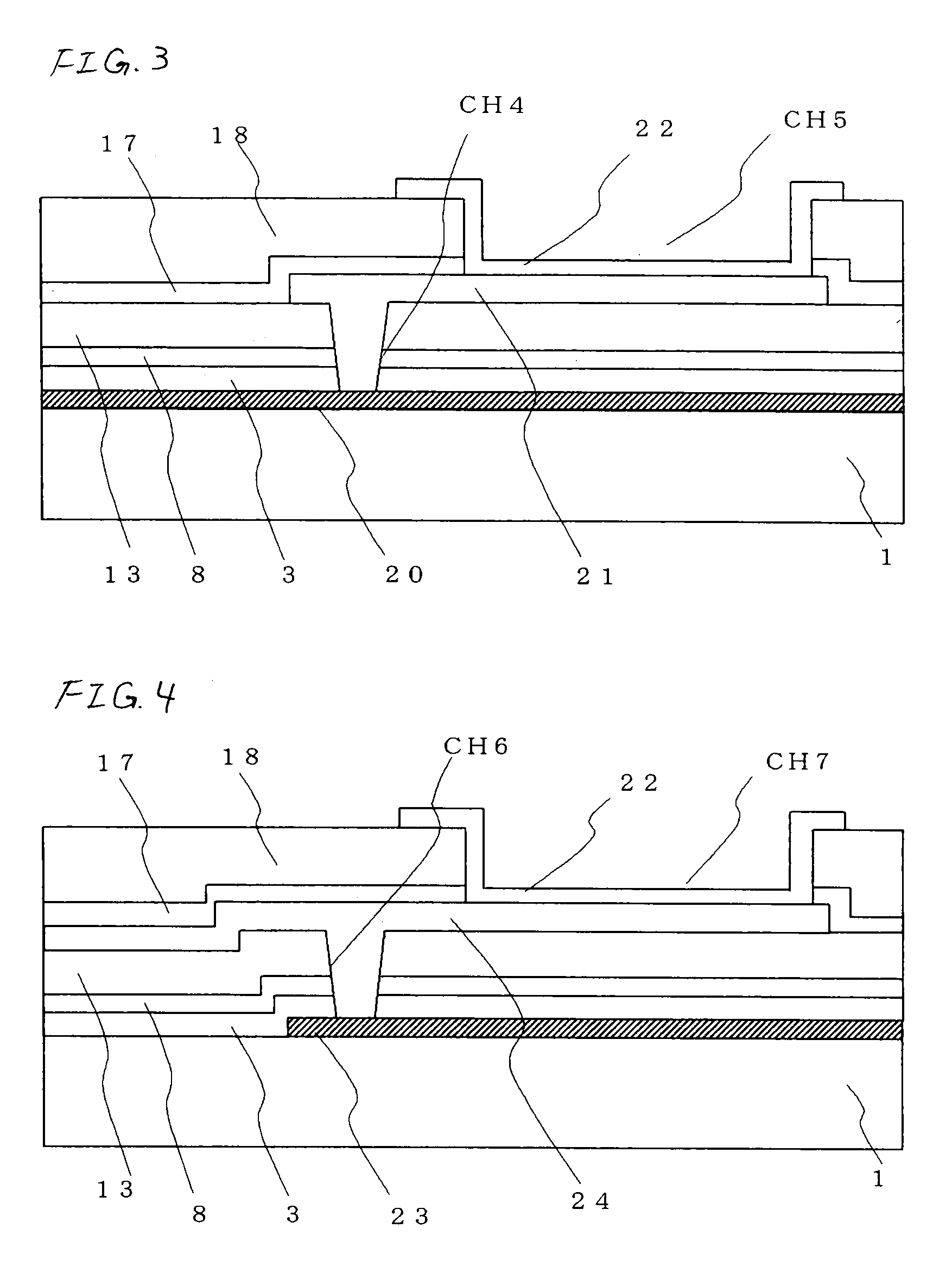
[0069]In the first embodiment, depending on an etching condition, there is a case wherein, in the processing for forming the contact hole CH1 that connects the drain electrode 7, which serves as the lower electrode for the photodiode 100, to the amorphous silicon film 9, a polymer may be generated by the element of an etching gas and be attached again to the drain electrode 7. In this state, when the P-doped amorphous silicon film 9, the intrinsic amorphous silicon film 10 and the B-doped amorphous silicon film 11 are deposited to constitute the photodiode 100, the adhesion to the drain electrode 7 is deteriorated and the amorphous silicon film might peel off.

[0070]According to a second embodiment of the present invention, a leak current of a photodiode 100 is inhibited, and an amorphous silicon film is prevented from peeling off. This embodiment will now be described while referring to FIGS. 9 and 10. FIG. 9 is a plan view of a TFT array substrate 200 provided for a photosensor for...

third embodiment

[0075]In the second embodiment, the lower electrode 25 has been formed so that the pattern end completely covers the contact hole CH1. This is because of the following background. Assuming that the lower electrode 25 is smaller than the contact hole CH1, the drain electrode 7 underneath will be exposed by etching the lower electrode 25. In a case wherein the drain electrode 7 does not have etch selectivity relative to the lower electrode 25, the drain electrode 7 underneath would also be etched. Especially when the connection portion 7a of the drain electrode 7 is etched, a wire break will occur between the thin film transistor (TFT) and the photodiode 100. Therefore, etch selectivity relative to the drain electrode 7 is required for the material of the lower electrode 25, and the selection range of materials is narrowed. To avoid this problem, generally, the lower electrode 25 is formed larger than the contact hole CH1. That is, the lower electrode 25 is formed to cover the contact...


PUM


Abstract

For a photosensor, an array substrate is provided, wherein the edge of a photodiode is enclosed by the opening edge of a contact hole formed on a drain electrode.

Description

[0001]This application claims priority from Japanese Patent Application No. 2007-127889 filed on May 14, 2007, the entire subject matter of which is incorporated herein by reference.BACKGROUND OF THE INVENTION[0002]1. Field of the Invention[0003]The present invention relates to a flat-panel photosensor that includes an active matrix type TFT array substrate, on which a photodiode for converting visible light into electric charges and a thin-film transistor (hereinafter referred to as a TFT) employed as a switching element are arranged like a matrix.[0004]2. Description of the Related Art[0005]A flat-panel photosensor that includes a TFT array substrate, on which a photodiode for performing photoelectric conversion of visible light and a TFT are arranged, is applied as a contact image sensor or an X-ray image display apparatus, and is widely employed. Especially, a flat-panel X-ray image display apparatus (hereinafter referred to as an FPD), which is constituted by providing, on a TF...

Claims


Application Information

Patent Timeline
Patent Type & Authority Applications(United States)
IPC IPC(8): H01L31/113G01T1/24
CPCH01L27/12H01L27/14603H01L31/022408H01L27/14612H01L27/14658
Inventor HAYASHI, MASAMIMIYAYAMA, TAKASHIMURAI, HIROYUKI
Owner MITSUBISHI ELECTRIC CORP
Why Eureka
Try Eureka